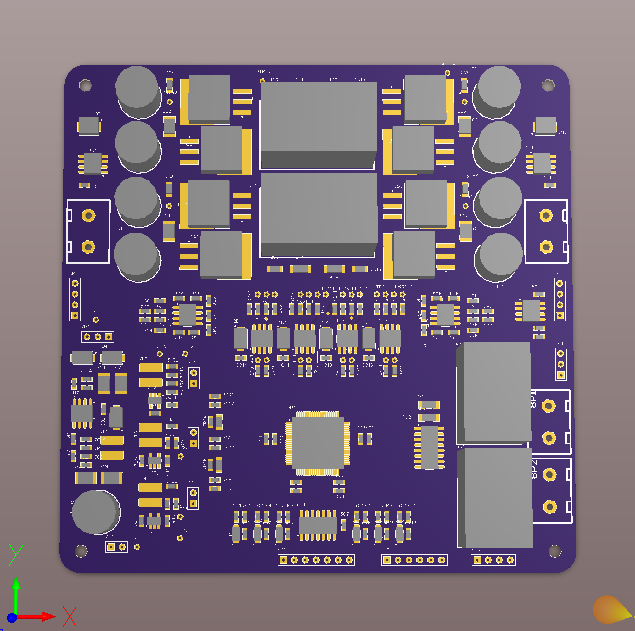
I have been pushing forward with the next PCB design where all elements of the system are combined on one board. I have included a screen capture of what the board will eventually look like. You can clearly see the two inductors for each phase of the buck boost power stage, surrounded by 4 Buck FETs on the left and 4 Boost FETs on the right. I am hoping to push this design out to get fabbed next week. Then I will be focusing back on writing code, getting some delrin laser cut to mount this in a pelican case with a battery, and building up a BOM for a parts order.

 Nathaniel VerLee
Discussions
Become a Hackaday.io Member
Create an account to leave a comment. Already have an account? Log In.