Just got the first boards back and with only a few minor schematic issues, the boards are successfully streaming the IMX219 across the GMSL link and can natively display the stream on the Raspberry Pi 5 (Pi 4 also works) with simply using libcamera.
Ideally and long term, these will be programmed by some type of driver but functionally they are sound.
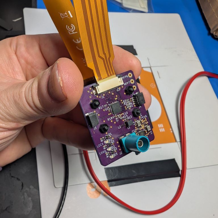
These were done on a 4-layer board from OSH Park and the controlled impedance guidance worked like a charm. I will detail layout in a follow up log but here is a picture of the working prototype before we dive into schematics.

Pretty decent soldering job on the first try, just needed to rework a few self-inflicted solder bridges. Great stencils from OSH Stencils.
On to the schematics.
The full schematics can be found on my GitHub repo.
The schematics may seem fairly simple because they are. These SerDes devices don't require much to get going outside of some basic connections. The majority of the work is in the layout which I'll detail in another log.
The EV kits for these parts also have full schematics but since they're EV kits, they have a lot more on the board than what's necessary so I optimized it down to be specific to this application.
The first page is the hierarchy of the design. This board is simple enough not to require a hierarchical design but I like to organize my schematics like a block diagram to allow for easier navigation. I can thank my first engineering manager for instilling hierarchical design best practices into me as a young engineer out of college.
Top level hierarchy of the design.
There are five sections of the design that are pretty consistent across all GMSL based designs.
- Connector - The connection to the outside world and to the deserializer.
- Power - Everything needs power, but you'll see a line from the connector because I'm using power over coax allowing me to transmit a few Watts of DC power on the same cable as the GMSL link further reducing wires.
- Peripherals - This is anything that you want to hook up on the bidirectional communication channel of the GMSL link. I put QWIIC connectors so folks can plug in whatever they want. But again, these are transmitted at a different frequency on the GMSL link reducing wires.
- Camera - That is simply the 22-pin connector for the IMX219 RPI camera but in reality, this is the input PHY that we are serializing on the link.
- GMSL - Best for last. This is the bulk of the schematic with the serializer. If you notice, the peripherals and camera both go into this sheet. This is because GMSL can combine both high speed and low speed data feeds on to the coax cable. Also, this is transmitted at microsecond latency.
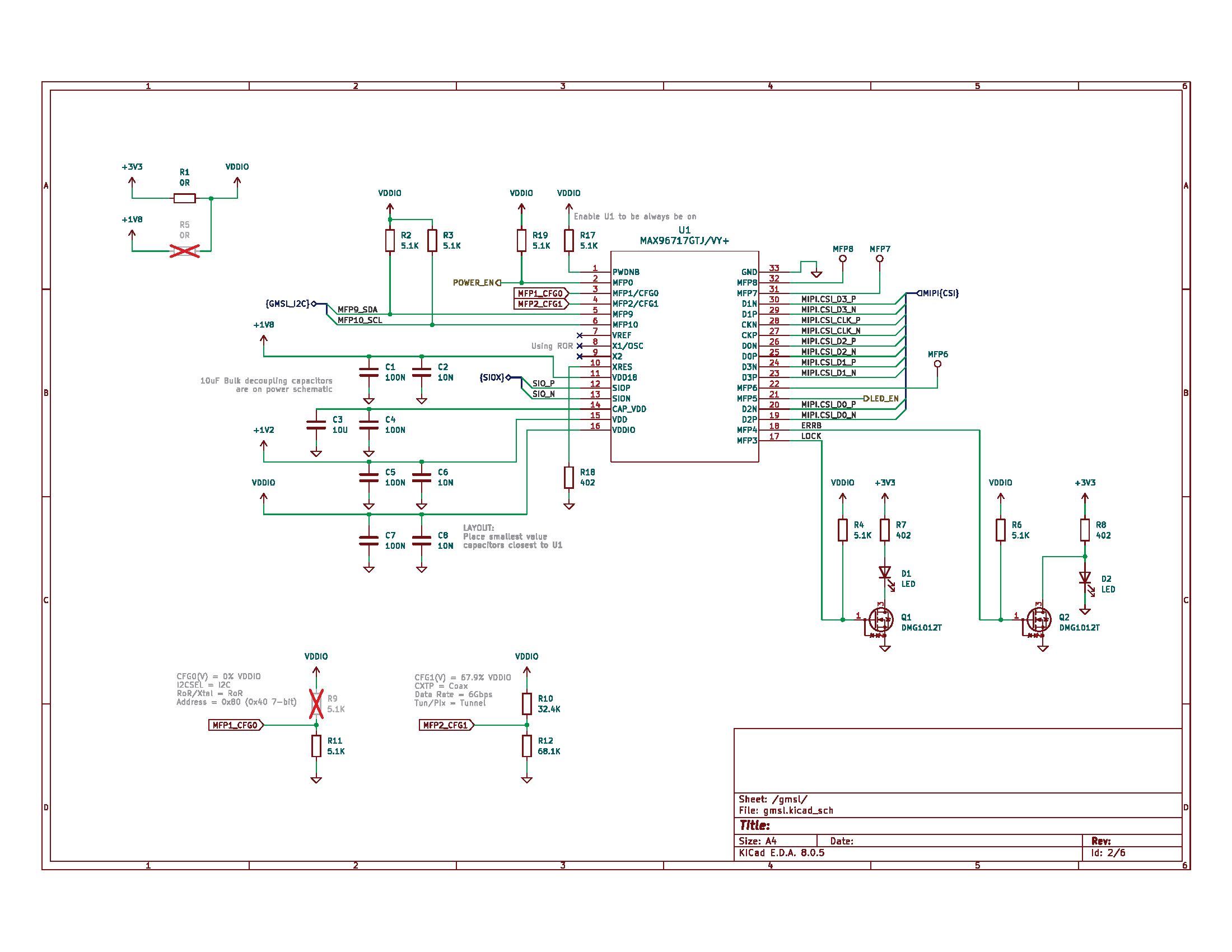
Let's just into the fun one first, the main GMSL schematic.

Not too much going on but let's start in the top right corner and work counter-clockwise. I recommend opening the schematic and following along. Note: minor fixes where made on the LED logic and power enable pin.
You'll see some testpoints labeled "MFPx", MFP stands for Multi-Function Pin and it's like a GPIO on steroids. Each MFP has... multiple functions that are specific to each device but they are mainly I2C, UART, GPIO, SPI, ADC, etc. capable pins that can be configured for whatever your application needs. You can also see MFP3 and MFP4 on the bottom right which are used to indicate that the GMSL link is locked and if there is an error on the device. Not mandatory to route these out but helpful for a quick visual indication of the link's health.
Next is the bulk of the layout and schematic planning, the MIPI-CSI2 interface. At first glance, it appears I completely messed up the pin connections however, these GMSL devices allow for lane remapping and polarity remapping. After talking to the layout engineer (yes, I talk to myself), these were the ideal connections to significantly simplify the MIPI routing. The only thing you can't remap is the clock lane but I could change the polarity which helped.
There are registers in the device that also need to be reprogrammed to remap these but I selfishly prioritize hardware simplicity over software complexity. The register programming is straightforward but doing changes like this require good coordination among the schematic engineer, layout engineer, and software engineer.
Onto the power supply, it is a simple combination of bulk and decoupling capacitors that is outlined in the datasheet. I made a note of the PCB placement to have the smallest values closest to the IC. The bulk capacitance is on the power page so I made a note of where they are.
You'll see one rail, CAP_VDD, which doesn't have a power feed but is needed to decouple the core VDD supply. The other rails are:
- VDDIO - (I chose 3.3V to support the QWIIC connectors but it can be any range from 1.8V to 3.3V). Always (please) have a discrete rail called VDDIO rather than using 1V8 or 3V3 for the GMSL logic. This is because VDDIO can change, which is fine, but if you miss something on the page that is pulled to this rail, you will have issues or burn up a part.
- VDD - which is the core supply and can be provided a voltage supply of 1-1.2V. I chose 1.2V since that is the typical camera voltage power supply and the PMIC chosen outputs that value.
- VDD18 - this is just the 1.8V device rail
Buried in these pins, you'll also see SIOP and SION. I'm not sure the exact acronym breakdown but I call these "Signal Input/Output Positive" and "Signal Input/Output Negative". GMSL supports both single-ended (coaxial) and differential (shielded twisted pair) configurations of the cable. These will be discussed on the connector page.
Next up is the XRES which is the 402 Ohm termination resistor for the PHY.
You'll also notice no-connects on the crystal oscillator inputs X1/X2. Typically, a clock source is needed to drive these parts but the newer MAX96717 has a feature called ROR allowing me to use the clock on the deserializer which is recovered from the GMSL link. This means fewer parts and easier layout, and no 25MHz radiating on my sensor board. If this camera has any GPS based devices near or connected to it, you'll know 25MHz likes to peek it head out right in the middle of the GPS band.
A few more MFPs on the part. MFP9 and MFP10 break out the main I2C channel that is then connected to the QWIIC connector. MFP0 is used for the power enable GPIO of the camera. PWDNB is the reset pin of this device, I have it pulled high to always have the device enabled but it could be controlled if desired.
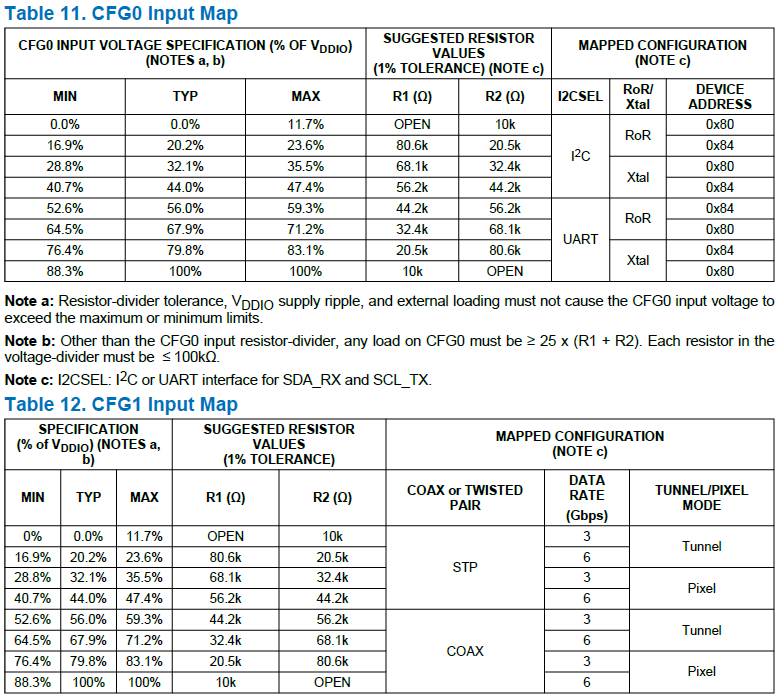
MFP1 and MFP2 have a unique usage as the configuration pins of the device and bootstrap the basic settings required for a GMSL link to be operational. I advise against using these unless it's a last resort because any noise on these pins could cause the part to boot in the incorrect manner. Lower in the page, you'll see the voltage divider and associated settings. I always try to be explicit in schematics with my bootstrap intentions. You'll see in the comments that coax, 6Gbps, I2C, RoR, tunnel and the I2C address of the device.
Here are the CFG values and what they configure.

The CFG0 and CFG1 configuration capabilities.
Lastly, you'll notice some interesting resistor values of 5.1kOhm and 402R used for multiple purposes. This was done intentionally to minimize the different BOM components. When I was a design engineer, different BOM values translated to more line items to manage, source, and worry about. 5.1kOhm as a pullup is more than sufficient for I2C or the FET gates. It is a required component value for the power over coax filter so I back propagated the value through the schematic. And coincidentally, 402R is actually a good enough value for the LEDs but a mandatory value for the GMSL device. So they're not random but meant to help simplify the design needs. You'll see these two values again on the power page.
A lot of detail on this page so I'll detail the other four pages in the next log!
 tom
tom
Discussions
Become a Hackaday.io Member
Create an account to leave a comment. Already have an account? Log In.