Took the step 0 for this project. I needed basic proof that I can pull this off. Basically a minimal implementation that can read a KiCAD board, process it and create something that tells me this will work. I am developing this first and foremost to work for me. Here is AtiVEGA with the results of today's work:
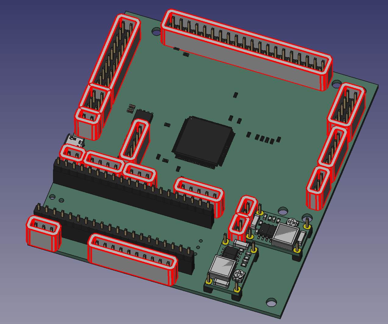
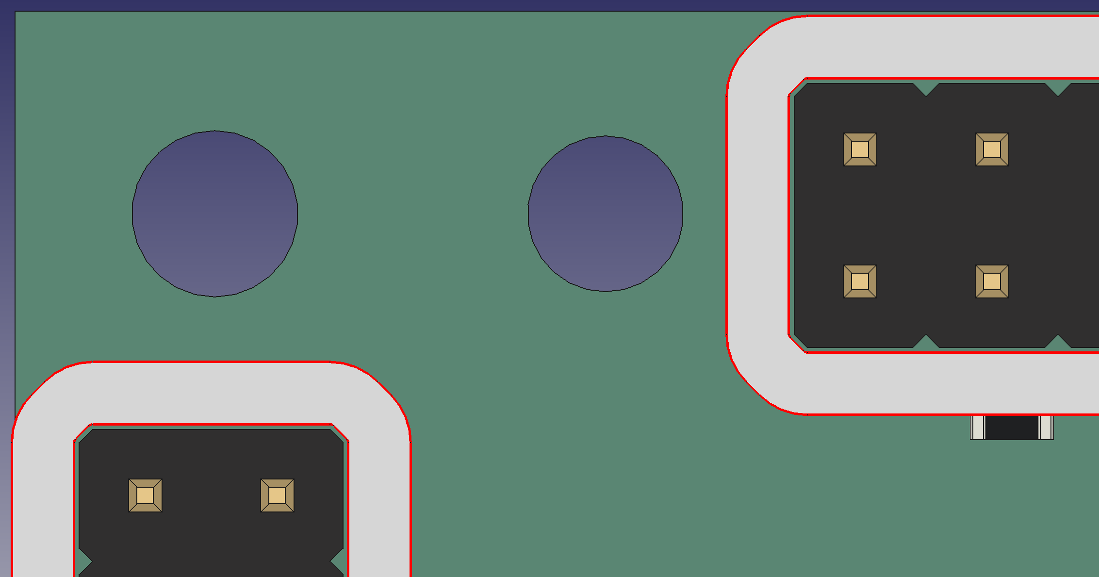
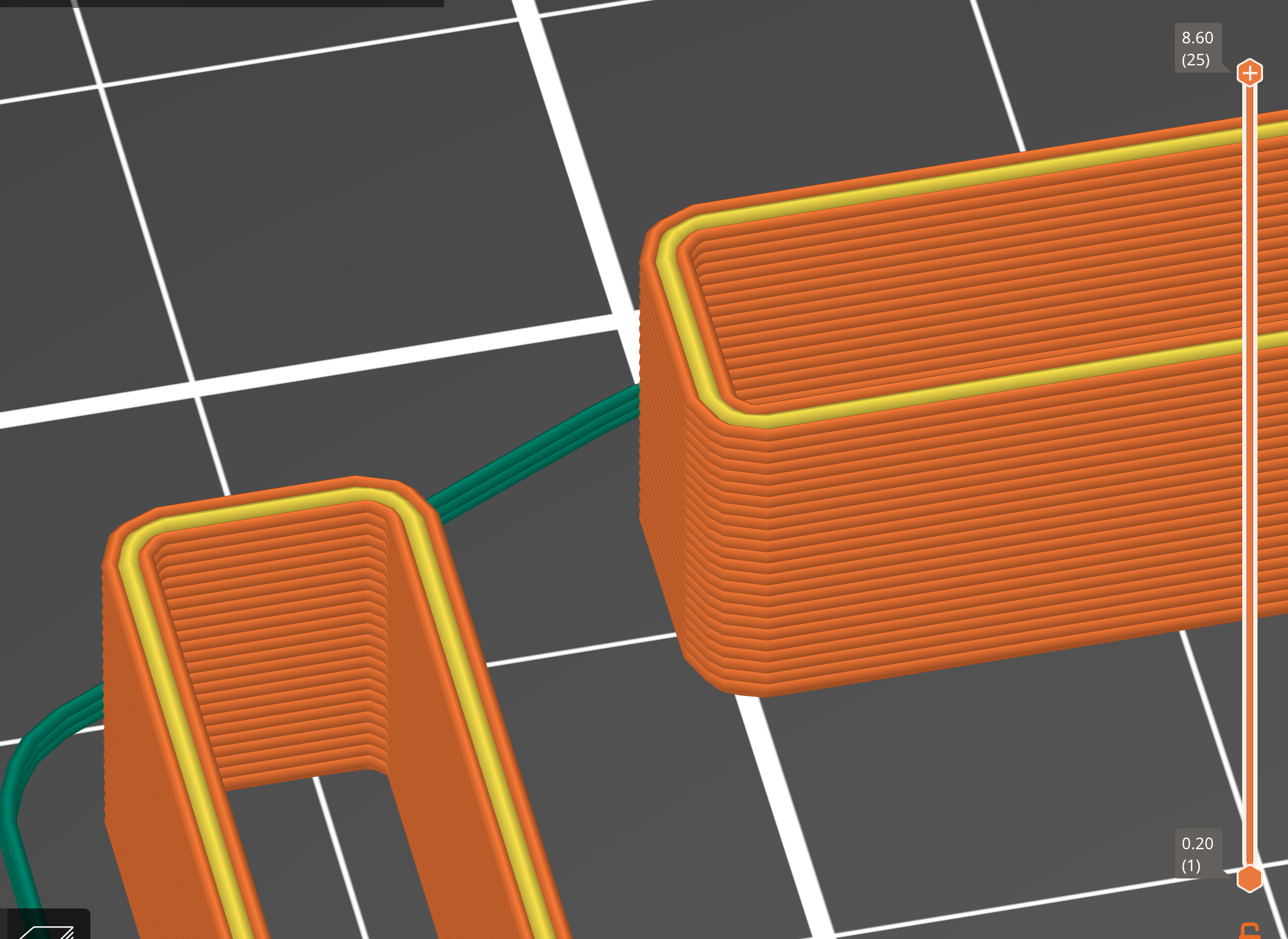
How does this work ? In short, my script iterates over all the TH components. Loads their 3D models. And transforms them to their final position on the board (notionally at least!). The simplest method to hold the TH components in place is with a simple shell, as shown above. But how do we compute the shell ?
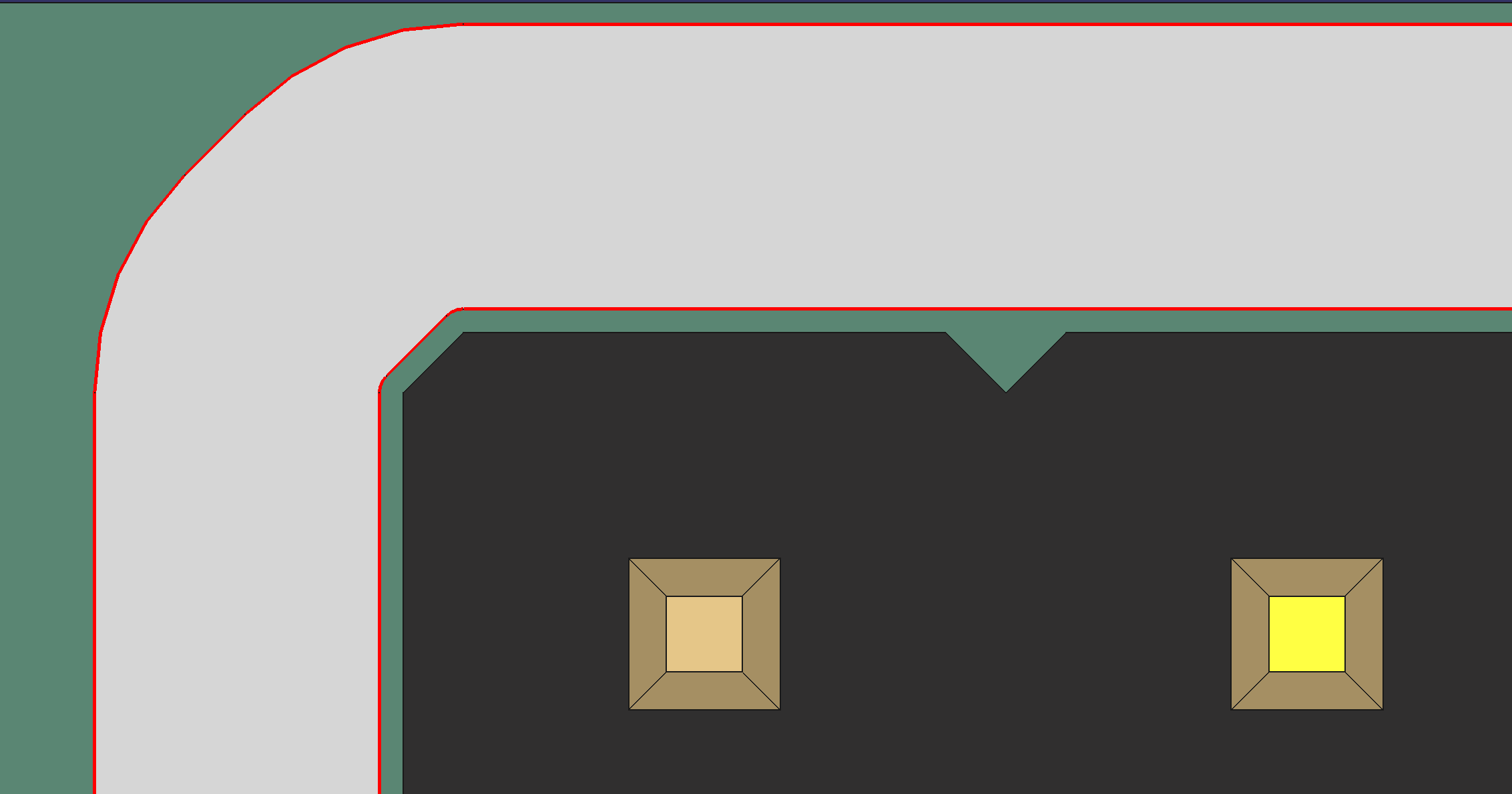
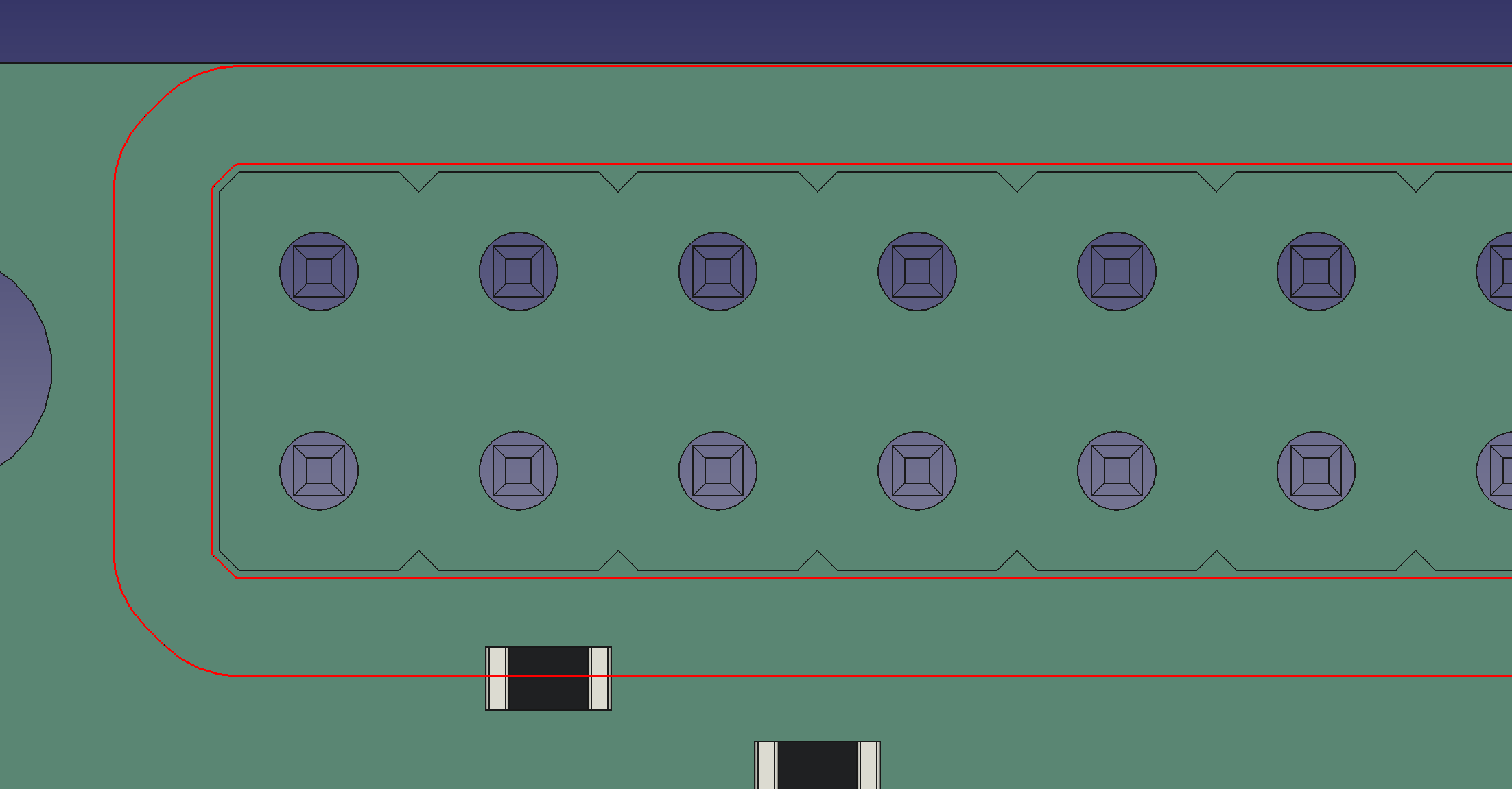
A simple method (KISS for now) projects the 3D model of the component (e.g. 2x20 berg header) onto 2D space - say the top layer. Just drop the Z components, that will do. As a result, you get a whole lot of (x,y)s - essentially points that represent the 3D model. Now, you take a convex hull. This is guaranteed to encompass all points. It also has a nice property that it wont "hug" the model in its nooks and crannies - e.g. the gaps between the 2.54 mm spaced plastic housing. The below picture in wireframe should make this clear.
Will this approach work for every component ? Definitely not. But does it have to - again not, at least initially. I'll probably include simple overrides at the component and footprint level so that the generic nature of the tool is preserved. That way, anyone using it can even make use of most of the generic functionality - and include their own overrides flexibly.
Now that step 0 is done - here are my next steps:
- close the holes with caps so that the components can slide in and sit (now, won't that be satisfying!). This is simple, and I can easily accommodate components of various heights.
- add a frame on which the PCB will sit. Need to dig into more "pcbnew" for this, and/or lookup stencilframer.
- merge the caps into the frame. A simple slab matching a bit more than the PCB shape will do, but it will be fun to come up with ways to save plastic in the 3D print ! Premature optimization is the root of all evil, says Knuth. But yet, me starts the think!
 Shree Kumar
Discussions
Become a Hackaday.io Member
Create an account to leave a comment. Already have an account? Log In.