Why Version 2?
Version 2 of the CCD-pos project is dedicated to an upgrade of the electronics and the software to improve the signal quality, hopefully with a better measurement resolution as result. The choice to galvanically isolate the frontend electronics to reduce noise on the signal, which resulted in a complete redesign of the electronics.
Version 1 was build on a number of built-in features of the MCU, minimizing the need for additional components. The STM32L476 has two opamps and two DAC's on board, which allowed me to invert and scale the CCD-signal to bring it in range of the ADC. This setup made use of the supply voltage of the MCU, being the +5V of the USB connection with the desktop PC that analyses the CCD-signals. As the power lines of a PC may carry unwanted noise and disturbances, I decided to separate the sensitive part of my setup from these sources of misery.
What are the consequences?
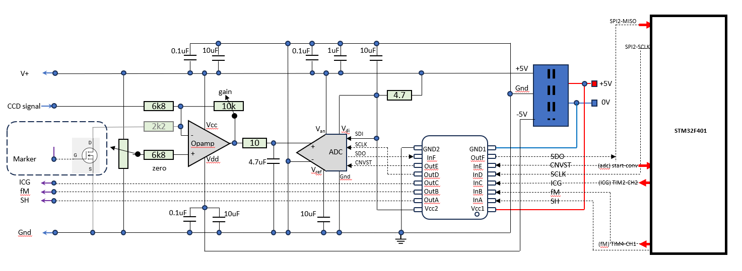
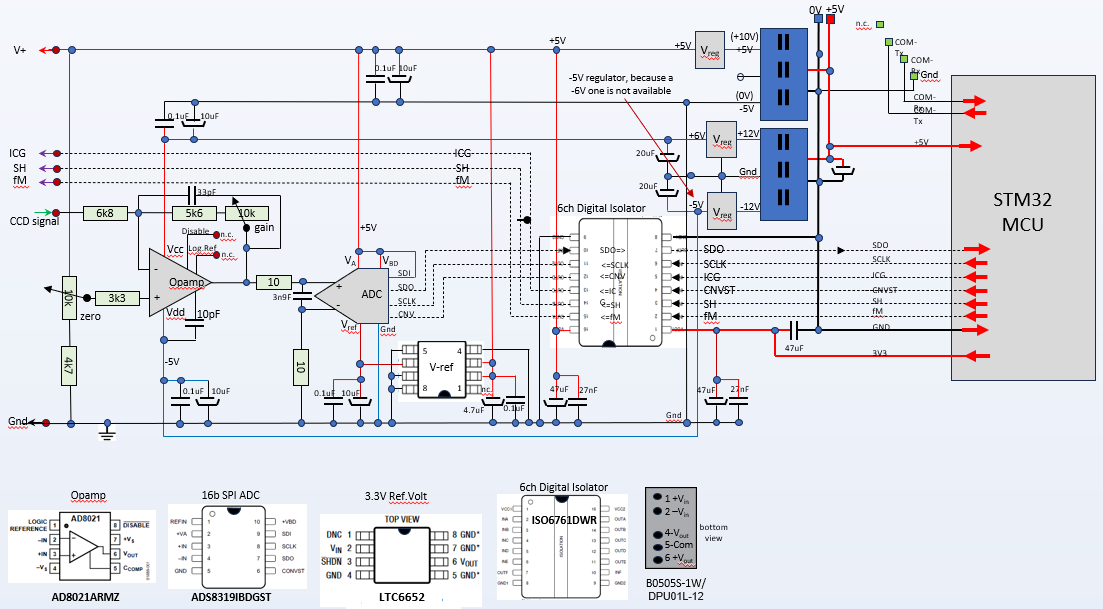
The three pulse signals for the readout of the linear CCD are generated by the MCU, so they just have to pass the galvanic isolation, for which there are dedicated IC's. But the output of the CCD is an analog signal, which is not easily transferred over an isolation barrier. The choice was either an analogue isolator (expensive, possible signal distorsion) or apply a separate ADC with a handsome digital interface on the isolated side. This approach modifies the transfer of the CCD-output to a regular digital isolation. The trade-off for an amateur like me was simple: a separate ADC with SPI interface which digital signals are transferred over the barrier. There are multichannel digital isolation chips for sale, even with the specs I needed: five signals from the MCU to the isolated side and one (the SPI MISO signal) in the opposite direction.
This was the global plan, which even looks to be feasible.... However, the hash reality learned me otherwise.
The selection of the key components for an affordable price appeared to be challenging. I have spent quite some time on searching the internet for companies that sell the chips I selected to private persons for a reasonable price. Plus preferably all IC's from one source to reduce the transport costs.
AliExpress considerations.
In a situation where the budget for a project is tight, a provider like AliExpress is seductive, certainly when the experiences until now are quite positive. The downside of AliExpress is its poor searching mechanism, at least to my opinion. I find it hard to trace and compare sellers of a potential product, with additional the "strange" algorithm for the transport costs. Sometimes the transport fee is hardly depending on the quantity one buys (understandable when the total weight hardly changes), but be not surprised when doubling the quantity makes the transport explode to 5x the fee for one piece. Also the cost ratio of product vs. transport may differ astonishing between the various sellers: one must always look at the sum of product + transport to determine if a seller really has an attractive price.
The first setup with galvanic separation.
From the previous, it may be clear I bought a number of new components from AliExpress sellers, from which only one product (a number of ADC's) appeared to be flawed. Unfortunately, because my specifications went into the "high-end" products, I could not buy all IC's I selected from China, so was forced to order those from European suppliers. In version 2.0 the WeAct-F401 board is still applied, with the version 1 Marker mechanism as option, see below:
After this design was realized on a piece of experiment board, it took me a long time and quite some modifications to get it working more or less like I wanted. The unregulated DC-DC converter appeared to produce an unacceptable pollution on the supply voltage, so I had to add voltage regulators to correct that. The three timing signals for the CCD readout were generated, but didn't arrive at the connector to the cable to the CCD (see project 'CCDpos version 1' for details). I had a terrible lot of troubles to make the digital isolation chip do its job: just send pulses from each input to the related output. Looking back, I guess I made mistakes with the two separate power sources (the primary, Vcc1 and Gnd1 resp. the secundary, Vcc2 and Gnd2) and got a kind of crosstalk between channels. Luckily, I had bought a very common, cheap Chinese 8 channel Logical Analyzer, that helped me to determine what was going on. Slowly I started to learn how to handle the digital isolator and that decoupling capacitors on the power pins for both sides are crucial for a good pulse transfer.
Tough programming challenges.
The next step was to find a way to: a) provide the ADC an appropriate trigger signal, b) generate the SPI CLK pulses for c) reading the output of the ADC into the SPI-MISO input. The principle was shown in the Datasheet of the MAX11160, the ADC I started with. See picture below:
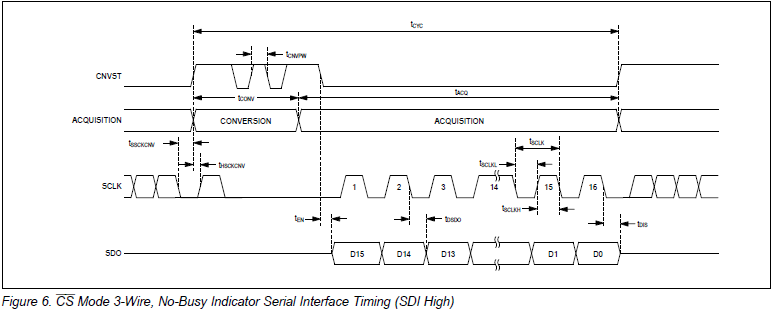
The ADC follows the voltage difference at its inputs (named here 'Acquisition') until the trigger input (named here 'CNVST') goes high. On that moment the ADC starts a 'Conversion' which is finished after max. 1.5us. From that moment the SDO pin of the ADC can output its 16 databits, but only when its CLK-input receives a train of 16 CLK pulses.
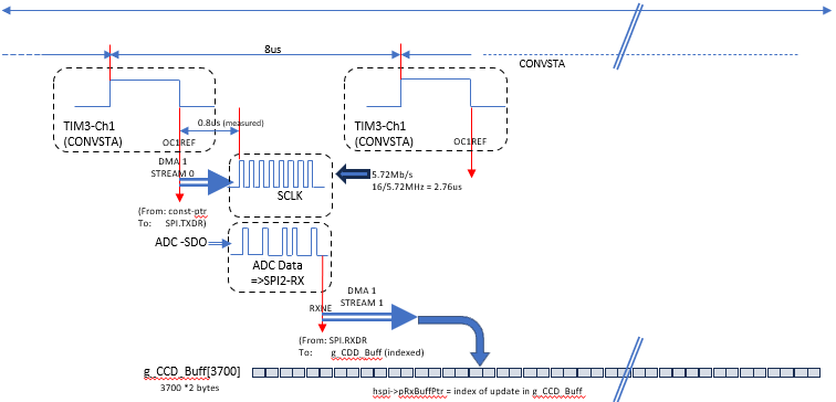
At first sight this mechanism seems not very difficult to implement, but the reality of programming a STM32F401 to make this happen is a different story, certainly for someone who is quite new in this area of programming. Luckily there is a STM Forum where people like me can ask for assistance to get things like this running. My experiences with this forum are fine, most of the times I got that much information that I managed to solve my problems. And so I learned a trick to make a SPI produce the CLK pulses I need to read the data from the ADC. When a SPI interface in Full-Duplex Master-mode is ordered to write a data-word to a client, it will generate the CLK-pulses, needed to export the data-package from its MOSI port. When configured for 16bits data, this means 16 CLK-pulses are sent from the SPI-CLK pin. When one configures the 'CNVST' pulse duration a tiny bit longer than the 'Conversion' takes, the ADC conversion can start by the rising edge and the SPI can start reading the ADC-data when 'CNVST' ends (on the falling edge). See the scheme below for explanation:
First stumbling around.
My first implementation was done with an interrupt (to make SPI transmit a word) and a DMA action (to read the data from the ADC). When I looked up this old code, it was clear I was searching for the right way of doing. There were quite a lot of lines with instructions for other approaches commented out, showing I didn't trust those statement(s), but also wasn't sure enough to delete the statement. The tip that a SPI interface creates the required CLK pulseswhen writing a word to another SPI compliant device appreared also more complicated than expected. There are a number of parameters for the configuration of a SPI, that allows a wealth of different ways to use a SPI interface. This makes it easy to make a wrong setting, causing no CLK-pulses at all (mostly) or a continuous stream of them (sometimes). It appeared to be a matter of remaining quiet and persistant, plus the help of my Logic Analyzer that finally learned me what the rules are.
Interlude on documentation.
In this context I want to express my annoyance concerning the documentation STM delivers, although it is a well known fact that writing good, clear documentation is a profession on its own. The bulky Reference Manuals (>2500 pages) for just one processor are helping to some extend, but seem written by technicians responsible for one or more sub-systems. This results in a tecnical correct (even that not always) description, which many times is not benificial for a user who tries to understand a mechnism and what statements are required to get done what he/she is intended to. I am not alone with my discontent on documentation: on the forum it is mentioned on a kind of regular base, also by guru's and other very capable members.
Following steps.
After the issue of SPI CLK pulses was tackled the following hurdle showed up: make the SPI interface receive the output words of the ADC. This appeared another stumbling stone, which took a lot of time to solve. There were a lot of variables that could cause the absence of data-pulses, which made my problem hard to solve. The fact I only had a two channel scope available didn't help either. I had ordered several identical IC's which all gave the same (bad) result. In short: this was one of the cases where AliExpress delivered a crap product. Whatever I tried, I never got reasonable pulses from the ADC and finally concluded it had nothing to do with my programming, it was a matter of bad hardware.
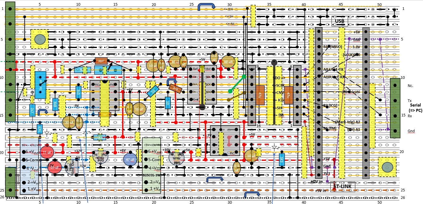
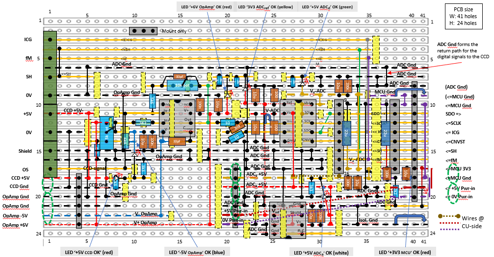
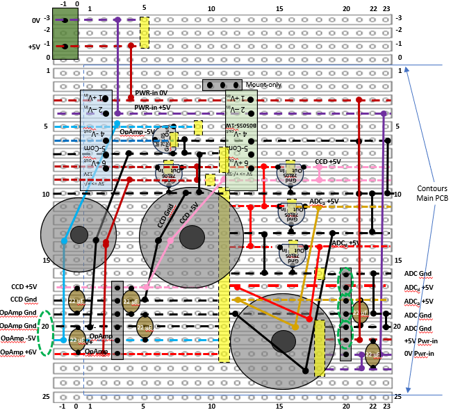
This conclusion had several consquences. I had to select and buy another ADC (my trust in the MAX11160 had vanished), plus all my experiments and changes on the experiment board had deteriorated the quality. So I decided to build a new board, with some changes in the layout, the implementation of the new ADS8319IBDGST ADC with 10 pins instead of 8, an additional chip (LTC6652) for the Vref of the ADC and LED indicators for the supply voltage. Of coarse, I needed to design and draw a new layout for this next version. As simple technician without electronic education I apply MS PowerPoint for this, see below for an example:
Example of a one board electronics design for the WeAct F401 MCU.
I tried to help myself with colored lines of different kind to distiguish the function of the traces to prevent errors The yellow rectangles symbolise cuts in the traces, the blue rectangles are resistors, the brown parts capacitors, the grey rectangles with black dots symbolize DIP-style IC-connectors. The solid vertical lines are pieces of wire on the component-side of the board. The black interrupted lines on the right are wires on the copper side of the board, they connect a selection of pins of the WeAct-F401 evaluation-board to my experiment.
When you look carefully to this new print you see two DC-DC converters and three voltage regulators, another step towards better performance by decoupling the voltage supplies for various components. I also tried to separate the three lines that carry the pulses for the CCD from the signal-handling parts of the board. On the upper side one sees a bunch of parallel black dot-stripe lines and a thick vertical black line between the pins of the isolation chip. They represent grounded traces and a copper ground-shield between the pin-rows of the chip.
Embarrasment as usual.
Of coarse (?) the commissioning of my new experiment print was a task on its own: I managed to have a short in one of the power-lines, causing an unrealistic high supply current. The presence of DC-DC converters and voltage regulators complicated the search for my mistake enormously. Finally, I ended up with desoldering the regulators plus removal of the IC's (easy with chip-connectors) and applying a voltage from a current controlled supply to measure the voltage-drops over (pieces of) traces. With this strategy and a lot of patience, I finally discovered I forgot to make a cut in a copper trace, that should separate a supply from ground, sigh!
Now, with all parts of the board working, it became possible to retrieve a conditioned signal from the CCD. As already explained in version 1, the TCD1304 sensor's signal is inverted with the 3.3V supply voltage as base. The applied opamp inverts this signal and has an adjustable reference for its second input to tune the 'dark current' level just above ground. I was quite happy to find this all worked as intended, so after some tuning the ADC was offered a nice signal to convert. And the investment of taming the SPI payed off as well, meaning the data-array in my MCU got filled with ADC-values! I considered this step forward a big achievement, as it meant I cracked the most difficult part of the challenge (which later on appeared not to be true).
New measurement equipment.
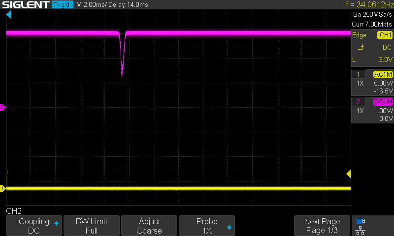
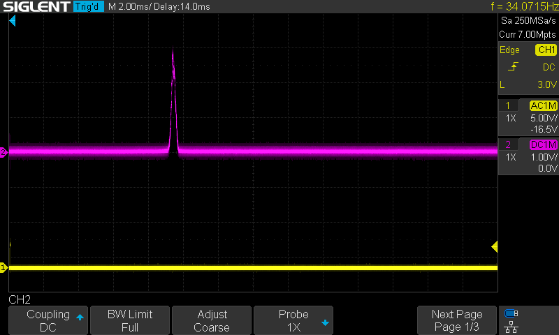
I do not remember precisely the moment, but around this phase of the project I granted myself a really big present: a 4 channel, digital storage scope with 1GS/s @ 2 ch, 500kS/s @r 4 ch, 200MHz bandwith and a 7" color display, plus the matching 16 channel 1GS/s Logic Analyzer extension. Working with these powerful devices made such a difference compared to the old 2 channel monochrome storage scope and a cheap separate logic analyzer, it almost became a joy to search for errors or bugs. As illustration I show some screenshots I saved. To be honest: these signals are measured in a later stage of this project, they serve as illustration of the digital scope capabilities only.
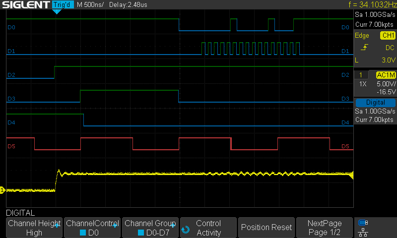
D0 = SPI-MISO pulses (ADC output)
D1 = SPI-CLK pulses (16 x)
D2 = ICG pulse for CCD
D3 = CNVST pulse: rising edge starts ADC, falling edge starts SPI-Read
D4 = SH pulse for CCD
D5 = fM pulse for CCD
1) Yellow = analogue signal of ICG (= D2), trigger
Last step to completion (or not?)
Up to the next and last step of the sequence: exporting the collected data by USB. This task was already programmed in version 1, so this software addition should be easy. Well, it was NOT. After quite some testing and trying why I didn't receive complete data-arrays, I became suspicious on the CPU load of the F401. I made some calculations about the tasks the MCU was requested to perform with its 84MHz clock-speed. I consider the chosen repetition rate of 30 readouts per second a minimum, so the ADC / SPI combi should handle 30 x 3692 channels per sec. The 'CNVST' trigger runs at 125kHz, so this means 125,000 times / sec. handling an ADC acquisition, followed by 30 times /sec. the output of 3692 U16 data-words, which equals 30*3692*2 = 221,500 bytes/sec.. I guess the ADC / SPI combi did not contribute much to the processor load, but the USB_OTG_HS interface appeared to consume too much CPU cycles to perform all tasks in time. I replaced the interrupt to launch the SPI-write for the equivalent DMA action to off-load the CPU, still not enough. Even after replacing the heavy-weight USB_OTG by a simple USART no complete data, so I had to conclude: I need another, more powerful MCU. This decisionn appeared the start of another, long period of tough struggle, disappointments and the need to be resilient.
A more powerful MCU.
When the step to another processor is inevitable, what does one choose? If affordable, not one with 50% or even 100% more speed, make a leap instead of a step. Looking around what is available (mainly on AliExpress), I found a candidate that looked really attractive: a 550MHz STM32H723VGT processor with significant more memory and storage on a WeAct evaluation board, with additionally a really small 4 lines LCD color display, for only 18.07 Euro! Supported by my previous experience with WeAct products I was not hesitant and bought such a board.
Dealing with another MCU board.
In comparison with the F401, the H723 board was much bigger and has on each side a 22 pin double row connector, so 88 MCU pins (!!) are exported. The difference in size made it impossible to incorporate the new board on the actual experiment print: although the height was sufficient, the width was too small. So it was obvious I had to build a new electronics board, already for the third time. But with the increasing complexitity of the power provisions, it would be more efficient to distribute the different functions over separate prints, connected by a (or two) connectors. And a logic extension of this design principle would be a separate carrier board for the MCU as well, allowing easy exchange of different MCU boards as long as the pin layout of the connector to the electronics remained identical (from a HW point of view of coarse).
A new setup with split functionality.
This different setup meant a redesign of the whole board layout to three separate boards. These prints were designed and built separately with as only constraint the positions and pin-layout of the connectors that finally links the boards together. I spent a lot of time at this combined design, to ensure that all aspects and limitations were handled correctly. This concerned:
- the integrity of the separate power traces,
- the most efficient position and pin functions for the connectors (in combination with 1 ),
- ability to stack the electronic board on top of the power board,
- feed-though of "noisy supply voltage" from the power- to the MCU-board,
- addition of LED indicators for every supply voltage,
- careful checking the validity of all traces,
- addition of "noisy" and "isolated" Ground connections for test pins,
- addition of a jumper to force a shortage over the isolation barrier for easy testing signals of both sides.
The investment of time and attention payed off by a rather short commissioning time, although I still have spent quite some time on details, like adding capacitors for better signal shaping and noise reduction. Below you find some pictures of the new pieces:
Version 4.0 of the electronics scheme, with the power components and MCU in simplified form.
|| pwr-conn || pwr-conn || MCU conn Layout design for the electronics board version 4.0, with three male headers on the copper side to connect the Power- and MCU-board.
Layout design for the power board version 4.0, with two female headers to connect to the electronics board. On the upper part is another three pin connector, which acts as a spacer for mechanical purposes only. The three circular objects on the power board represent ferrite cores where some power lines plus their returns were wound on in bi-/tri-filar mode to suppress common mode fluctuations.
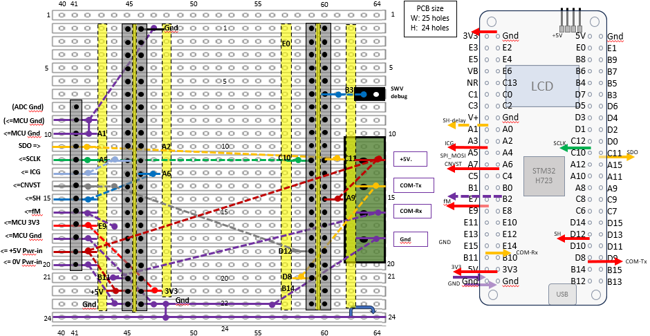
Layout design for the MCU carrier, with a female header to connect to the electronics board.
All pins of the double row connectors are separated from each other and have a small piece copper trace to allow soldering wires to the female connector on the left side.
Programming the H723 MCU. ===============================
My selection of the STM32H723 MCU appeared to be a choice "not hindered by any knowledge". It is one of the high-end products of STM that brings a number of "new features", meant to offer advantages, but at the same time posing serious challenges to the programmer by adding complexity. On top of that, I suffered from still being a newby in the world of MCU programming, plus the "bad documentation issue", so I had to consult the STM forum again.
This time the stumbling stone was the newly introduced 'DMAMUX': a mechanism that allows almost every device within the MCU to "fire" a DMA action. I skip the period of confusion, irritation and sometimes happiness when receiving assistance. One of the kind guru's on the forum told me: "you are trying to run, while you barely can walk". The end of the story was I learned how to deal with the DMAMUX to get the DMA actions I need performed. A big thanks to the patience of the guys who helped me.
My usage of CUBEIDE HAL-functions.
The HAL libraries in the CUBEIDE environment offer a bunch of high-level functions for all kind of actions with devices. For instance, there are different ways to use a timer, often with a further differentiation: I apply timers in PWM (Pulse Width Modulation) mode, where the signal has a frequency or rep-rate (often fixed) and an adjustable Duty-Factor, (a variable pulse-length between 0 and 100% of the period). The mode of control (further differentiation) can be chosen by selecting the function that starts the device: by polling (simple, but CPU hungry), by interrupt (more complicated, less but still CPU usage) and by DMA (more sophisticated and difficult, but no CPU load).
It is obvious I chose the challenging DMA option for frequent occuring actions, to save available CPU cycles for other tasks. The first subject was the timed SPI-write action to let SPI generate a set of CLK pulses, as explained earlier. I took the HAL-function: 'HAL_TIM_PWM_Start_DMA( .... )' as base. When you look into the code of this function, you see an enormous set of validity checks and statements to detect what the programmer wants to achieve. Because CUBEIDE tries to make its HAL libraries fool-proof, the code often takes 3..5 times the number of lines that are strictly necessary in a beforehand known environment and context. Experienced users hate this approach and call the HAL-concept 'bloat-ware'. Nowadays I follow an "in-between" approach: I use the HAL-function as concept for my intended action, but delete all checks and cases that predictably never will be executed. When I know in advance I use channel 1 of a timer only, it is an useless waste of CPU cycles to run a switch with 6 cases to detect the channel. Often I name the resulting 'lean' function "My_<Original_Function_Name( ... )>", with an additional comment header when needed, for instance when the list of arguments is modified.
In this case of 'My_HAL_TIM_PWM_Start_DMA( .... )', I apply another trick I learnt from one of the forum guru's. While the function primarily is meant for easy modification of a PWM's Duty-Factor (each update of a specific variable will be transferred by DMA to the timer's CCRx register - the pulse length). BUT the trick is: this DMA action can be repacled by another, completely unrelated DMA action, like writing a dummy value to a SPI register for the output of values via its MOSI pin. When this is configured and started, the Timer will cause the SPI interface to write dummy values (that are discarded) AND synchronously a set of CLK-pulses, without any CPU action required! Because the resulting fuction was derived from an "official HAL-function", the issues with the DMAMUX were handled "under the hood" in lower-level HAL-functions, so I bypassed the coding for it.
The configuration of the DMA transfer of data the SPI interface reads from the ADC is done really low-level, just by setting (sets of) bits in Registers of the SPI and the relevant DMA_Stream. It has taken me some time to reach the level of understanding how to do this so called "Bare Metal" programming, plus the knowledge what the real meaning of each register-bit is, but after the usual mistakes, the SPI-Rx function transfers the received ADC data to an auto-incremented index of the Data-array. Below you find my direct register programming to configure the SPI-Rx function by DMA.
    hspi3.Instance->CFG1     |= (1UL    <<  14);            // enable Rx-DMA for SPI3

    DMA1_Stream1->CR   =    0;                    // clear DMA1_Stream1->CR
    DMA1_Stream1->CR  |=    (0b00UL    <<  6);                // DIR=00: data transfer 'periph=>mem'
    DMA1_Stream1->CR  |=    (1UL    <<  8);                // CIRC=1: circular mode
    DMA1_Stream1->CR  |=    (0UL    <<  9);                // PINC=0: peripheral increment mode disabled
    DMA1_Stream1->CR  |=    (1UL    << 10);                // MINC=0: memory increment mode enabled
    DMA1_Stream1->CR  |=    (0b01UL    << 11);                // PSIZE=01: peripheral data size = 'half-word'
    DMA1_Stream1->CR  |=    (0b01UL    << 13);                // MSIZE=01: memory data size = 'half-word'
    DMA1_Stream1->CR  |=    (0b10UL    << 16);                // PL=10: priority level = 'high

    DMA1_Stream1->NDTR  =    (uint16_t)CCD_BUFF_LEN;            // data length for DMA1_Channel1
    DMA1_Stream1->PAR   =    (uint32_t)&(hspi3.Instance->RXDR);    // data source for DMA1_Channel1
    DMA1_Stream1->M0AR  =    (uint32_t)g_CCD_Buff;            // data dest. for DMA1_Channel1

    // Select TIM3-CH1 as DMA Stream1 request source in DMAMUX.
    // Note: DMAMUX channel numbers are slightly confusing in
    // the documentation. They aren't reliably 0- or 1-indexed.
    DMAMUX1_Channel1->CCR &= ~( 0x7FUL );
    DMAMUX1_Channel1->CCR |=  (DMA_REQUEST_SPI3_RX << 0);

    DMA1_Stream1->CR  |=    (1UL    <<  0);                // enable DMA1_Stream1

    // Start SPI3:
    hspi3.Instance->CR1     |= SPI_CR1_SPE;                // enable SPI3
    hspi3.Instance->CR1     |= SPI_CR1_CSTART;                // start transfer
A lot of testing, cq debugging depended on the build-in debugger, where I encountered another problem, especially with the DMA-related registers.
Inconsistent Register naming.
A very annoying documentation issue appears to be the lack of consistency in the naming of registers. This appears to be a long lasting problem, where forum members complain about for years (!!) already. The Reference Manual contains at the end of almost every chapter a structured list of the Registers for the described peripheral. In many cases the printed names and the names in the program code are not 100% identical, but the rules for mapping are often intuitive enough to coop with. However, in some cases this is NOT true, like with DMA and DMAMUX. And on top of that, the Register names the build-in debugger uses, c.q. requires for these devices are a matter of guessing with a rich fantasy.
On top of the problem to find out what Register name the CUBEIDE debugger expects (a requirement to view the Register value), there is another, already long-lasting bug. Sometimes the debugger seems unable to parse a VALID Register name and shows "Failed to find variable" (or something like that), which is the same text as when you enter an INvalid variable name. It looks a kind of gamble what the debugger presents after each start: the Register value or the dreaded complaint text. This implies that when I searched for valid Register names by trial-and-error, it may have been possible I entered a valid name, but rejected it because the debugger suffered from its bug!
Progress towards a working application.
In fact, the remaining part of the code was more or less identical to what I used for the F401 MCU, so the phase of testing the application on the new H723 was near. That's what I thought. But although it really looked like the data-array was updated and exported, not a single byte came out of the USB cable. Even worse: after the (re-)start of the application no Virtual Com Port (VCP) was added in the Windows Device Manager, meaning something basic went wrong.
After some attempts, I decided to change tactics and created a seperate test application that just should export a "Hello world!\n" string by the USB_OTG_FS peripheral. When this small dedicated test-program failed also, I didn't know what to do. I did a short attempt to understand the functionig of the USB_OTG peripheral, but stopped after reading 2 or 3 pages full with unknown acronyms and concepts, I realized this peripheral is way too complicated for me. Next I searched the internet for similar experiences, with the hope someone else has described how he/she had tackled this problem, also without success. A request for help on the STM forum learned me that debugging the setup of a USB connection is impossible, because it works with tightly timed commands and responses, impossible to trace with a debugger. It should work 'out of the box' and failure is likely a matter of HW problems.
So I ordered another WeAct H723 board on a 'quick delivery' condition, hoping that replacement of the faulty one would solve the issue. A week later I could replace the alleged failing board, to find out the new board behaved identically !! This was really not expected, apparently my trust in AliExpress products was unjustly. Of coarse I didn't want to give up my project, certainly not in this final phase of development, so I took the step to order an official STM NUCLEO-H723ZG development board. This time I ordered from a Dutch firm, to be sure of a genuine STM product, plus the advantage of a short delivery time, but at the price of twice the cost of a Chinese WeAct board.
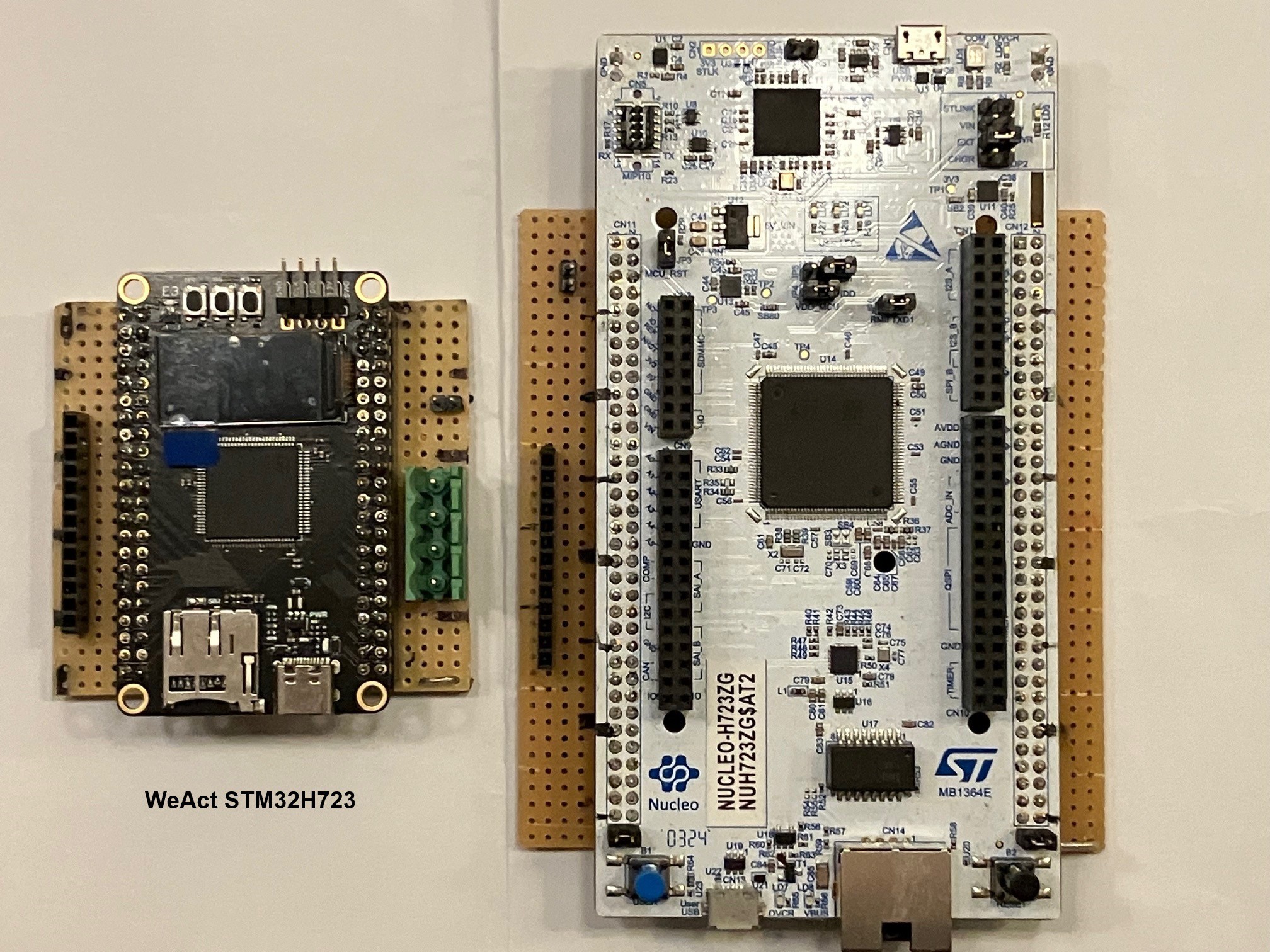
On the picture above one sees the big difference in form factor of these two boards, plus the difference in exported pins: the WeAct board has 2 double rows of 22 is 88 pins, the NUCLEO board has 2 double rows of 37 is 148 pins, plus a wealth of jumpers and solder bridges to allow many different configuration to be realized.
Now my decision to split different functionalities to seperate boards payed off: I only had to make a new MCU carrier print to accomodate the NUCLEO development board. On the left side of each brown carrier board you see the 13 pin header to connect to the electronics board.
Unbelievable: the NUCLEO board appeared to be equipped with yet another type USB connector: an USB Micro-B. Luckily I had an USB-A to USB-Micro B cable in my collection, so the show could go on. The first test I did was porting the USB_OTG test application to the NUCLEO board to see if the test string became exported. And YES, my desktop PC showed a new VCP and the application Putty displayed the "Hello world" strings!! Finally I can proceed.
Consolidating the new achievements.
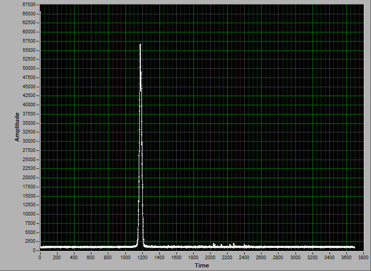
I ported all project specific files from the WeAct-H723 version to a new NUCLEO-H723 project. There were some minor issues, but soon I could run the complete application, including the export of the data, without problems by an overloaded CPU. The graph below is just a representation of the received data:
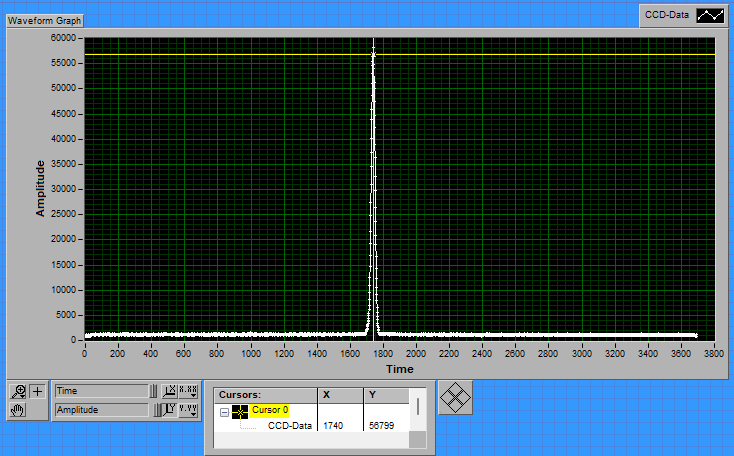
A remark: I had to put quite some effort in the tuning of the laser and the optical system to get a nicely shaped, narrow peak as shown. This part of the project certainly needs an improved, more rigid design to ensure a stable, good quality beam of light. The almost flat baseline is probably the result of the better signal-handling and measures to reduce noise, it looks like that aspect of version 2 is a success!
WeActH723 boards and USB_OTG - part 2.
The annoyance of yet another type small USB connector had a positive consequence. In my struggle to get the data-export by the USB_OTG peripheral working on a WeAct board, I changed the software and I replaced the board without success. But only now I realized I didn't switch the USB cable that connects to the desktop PC! What if ..... So I uploaded the very simple test program again to a WeAct_H723 board and repeated the basic test with another USB cable. And discovered there was no problem at all: both WeAct boards neatly delivered the "Hello World\n" strings to the desktop! Another lesson learnt: one must check every link in a chain before drawing conclusions.
With the knowledge that the WeAct_H723 boards are functioning, I certainly want to switch back to these smaller boards. However, I will delay this change until I feel confident the whole setup is functioning as I intend.
Markers again.
Already in version 1 of this project, I struggled with the identification of pixel 0 in the stream of bytes the desktop PC receives. With the much slower F401 MCU, the interval between the last exported byte of a set data and the first byte of the next data-set was rather short. In case the sequence of reading bytes from the VCP encountered an interruption, it was possible the desktop application looses the synchronisation. And because the displacement measurement is entirely based on the "distance" (number of pixels) between the center of the laser peak and pixel 0, it is essential to identify pixel 0 without any doubt. With the much faster H723 and outsourcing of most frequent actions to DMA, the data-stream became a sequence of fast bursts of bytes (3692x2bytes every 30ms). And because each burst starts with the 2bytes of pixel 0, the recognition of pixel 0 should be a piece of cake, albeit not 100% certain.
This easy solution was wrecked by myself: initially I configured the MCU software to generate an interrupt when the data-array was completely filled with new ADC-values. The Interrupt Service Routine (ISR) called on that event, simply invoked the USB_OTG function that exports the content of the data-array to the USB-port, and so to the VCP on the desktop PC. However, the CUBEIDE software also supports an interrupt that is generated when the first half of the data-array is filled with new data. When one configures both interrupts and adds a bit more intelligence to the ISR to distinguish the kind of interrupt calling it, the application can output one CCD readout in two consecutive (half-sized) streams of bytes, spreading the CPU load more equal in time. With this mechanism, the receiver program on the desktop is unable to distinguish which of the two streams contains the ADC-value of pixel 0.
To coop with this self-inflicted problem, the application edits the first three entries of the data-array, every time just before the first half of the array is exported. These entries are modified to a predefined 'Marker' pattern, being 0xFFFF, 0x8FFF and 0xFFFF, which is very unlikely to occur elsewhere in the data. The receiver program verifies if a retrieved set of data contains the 'Marker' values (in fact, the six bytes 0xFF, 0xFF, 0x8F, 0xFF, 0xFF, 0xFF) to identify the position of pixel 0. When the 'Marker' pattern is not detected, another chunk of bytes (0.5 x array-length x 2 bytes/word) is read and checked. Once the synchronization is established, the completion of the dataset will be straight-forward. Normally, the retrival of following datasets is a matter of reading the correct number of bytes, but the position of the 'Marker' is verified in every dataset for certainty. Although this strategy obscures the ADC values of the first three pixels, no relevant data will be missed as the CCD's output sequence starts with a set of dummy pixels.
Improvements of CCD pixel signal quality.
When playing around with the CCD output peak signal in relation to displacement of the roof-prism, I came across several issues to take care of. One is related to the behaviour of the optical system that defines the spot of light on the CCD-array. It appeared not trivial to create a situation where the intensity of the spot (= the amplitude of the ADC data) is stable for all pixels of the CCD. This issue requires better holders for the optical components, with provisions for precise and stable adjustment, which will be part of the next version.
The second one is the relative sensitivity of the CCD pixels. When I zoomed in on the peak in the received data, I saw the datapoints were not on a smooth line. At first I considered this due to noise on the signal, but the deviation of each pixel appeared to be related to its position in the pixel-array. When the peak position is slightly shifted, the deviations remain about the same height and on the same place. The only explanation for this is the sensitivity of the indiividual pixels. The datasheet specifies a figure for this "Photo Response Non Uniformity" with only a maximum value of 10%. This figure is defined as "the deviation of the signal of a pixel w.r.t. the average of all pixels @ identical illimination, divided by that average".
I already worked on a test application which measures and administrates the amplitude of the pixels in the peak at a certain position N times and than moves the position m micron. All data is dumped in a file for off-line analysis. This analysis of the collected data should provide an array of correction factors, one for each pixel. This correction-array can be implemented in the MCU code to perform a sensitivity correction before the data is exported. The measurement of these data requires a stable, reasonable constant peak over the whole measurement range, which I have not achieved yet. So this improvement also has to wait for version 3, which concerns a major rebuild of the mechanics and the optical system.
What next?
Like I already mentioned before, the remaining issues are mainly mechanical improvements, and a research project on its own: development of a nice, stable light source, plus the optics to transport the light to the CCD. I'm not sure yet which of these two items will become 'Version 3', although I have a feeling that the light-source and optics have a preference.