 Stephen Holdaway
After letting this project rest for a good 15 months (with occasional tinkering), I've picked it up over a weekend, verified the new schematic with its shift-register + LED driver configuration to drive the common-cathode 16-segment displays is sane, and completed the layout for the new board.
Since the last update I posted here, the main changes have been:
- A 20 pin STM8S microcontroller is now on the board to manage the display. This is probably overkill, but I have a bunch of these parts lying around, so figured I'd use one.
- The shift registers controlling the segments have been replaced with 74HC595Ds, since these don't need to sink much current. Digits are still sunk by the more expensive TPIC6B595Ds, since these need to handle up to 400mA when all segments in a digit are on.
I was unsure all of the driver circuitry was going to fit on in the limited space there is around through-holes, but managed to get it all in:

Coming back to this project fresh also let me pick up a few mistakes:
The two PORTB pins on the STM8S003F3 are "true open-drain" pins that don't have the ability to run in push-pull mode (ie. source current).
I've added high value pull-ups to both of these pins so they can drive logic levels.
The 74HC595s enable each segment's LED driver by sinking its GND pin, but will provide +5V to this pin when not sinking, rather than being high-Z.
Applying 5V to GND shouldn't be an issue unless the driver's +Vs sags or there are spikes on its GND at +5V that create a significant reverse voltage. The BCR402W datasheet states an absolute maximum rating of 0.5V reverse on any terminal, but in practice I've seen no adverse effects testing this on the bench for 30 mins at 5V reversed (which is 10x the reverse voltage than I'd expect to see in this circuit). With reversed polarity I can't detect any current until 9.63V, where 50 nA flows, and at 32V only 1 mA flows.
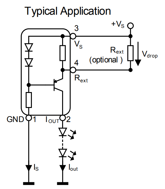
If this diagram in the BCR402W datasheet is actually representative of its internals, the reverse voltage tolerance of GND to +Vs should be greater than 0.5V - probably limited by the emitter-base breakdown voltage of the PNP transistor (typically around 5V). I'm fairly confident these aren't going to explode suddenly from small excursions past the 0.5V limit in the datasheet, but if segments begin to quit I'll have a possible culprit.
Also:
- The NPN BJT on the buzzer was wired up as PNP in the original layout.
- Segments 11, 12 and 13 were misaligned vertically by 0.5mm in the original layout.
The rev 2 schematic now looks like this:

After another round of checks, I'll send this off to the fab!
If I've screwed something up this time around, it should hopefully be possible to bodge, unlike the previous disaster.
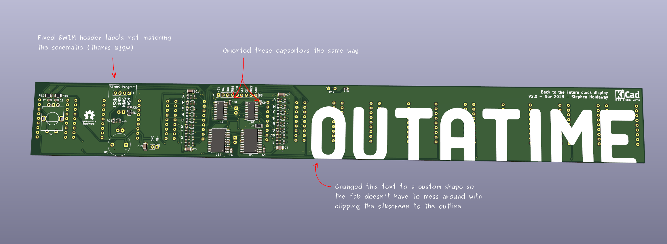
Edit: I made some last-minute mistakes on the silkscreen which I picked up after ordering, but fortunately I'd made a typo in the fab's submission form, so they rejected the order. The submitted board now looks a bit tidier:
Discussions
Become a Hackaday.io Member
Create an account to leave a comment. Already have an account? Log In.
I wonder about your STM programming header. Silkscreen doesn't match the circuit?!
Are you sure? yes | no
Darn, welll spotted - I rewired that header at the last minute to match STM's recommend SWIM header, but as I was working in high contrast mode where the silkscreen is greyed out, I missed changing it!
Are you sure? yes | no
You're welcome! I try to make silkscreen check a habit now, because I have mislabeled Rx/Tx and the like tooooooo damn often!
Are you sure? yes | no