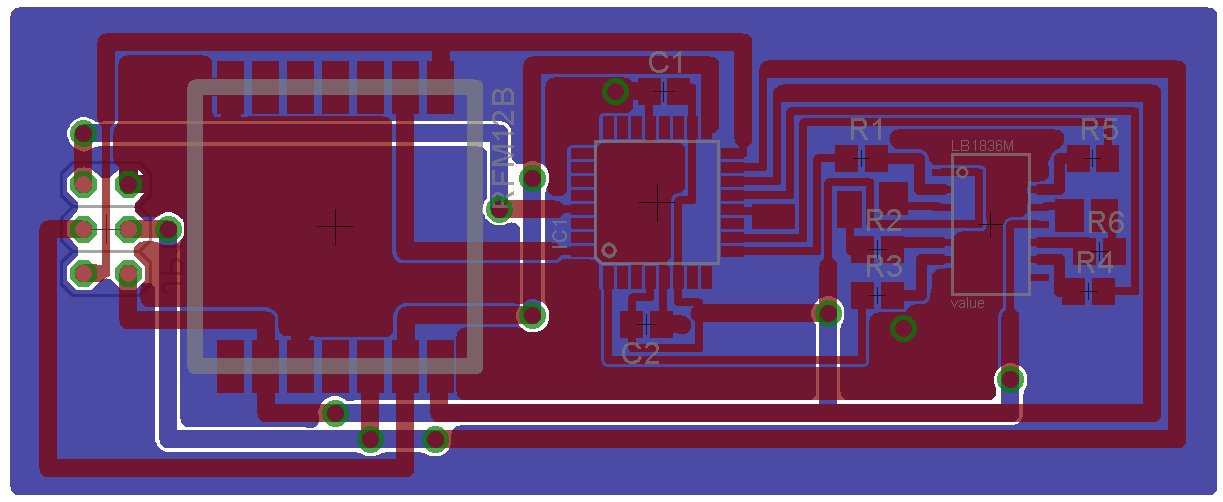
The current state of the project is that I have a working breadboard implementation of the circuit, and all the firmware seems to be working as well. The last week or so I entered the schematic into EagleCAD and designed a PCB based on that. So I am now ready to start fabricating the PCB. I can say with confidence this is the most challending PCB I attempted to create at home yet. When working in the cad software it looks fine, but when I printed the layout (on paper, just to check) I realized it is TINY! Apart from the ISP programmer pinhead, all components are SMD's. The entire PCB is about the size of a stick of gum. I'm glad I made a UV exposure box a while ago. This would have been quite impossible to fabricate with the toner transfer method I used previously. It's a 2-layer PCB as well, although I deliberately made the bottom layer such that it can be easily done using a few wires instead. Here is the final result:

Hopefully I can show the final product in the next update.
 Jeroen
Discussions
Become a Hackaday.io Member
Create an account to leave a comment. Already have an account? Log In.