 Eric Lind
Disclaimer:
When I started this journey down the 6809 path I had never heard of the TRS-80 or any of its siblings, I'm European and very much loyal to Commodore, with both C64 and C128 on the desk. In later days I started tinkering with Z-80 and ended up getting 2 Speccys (Sinclair ZX Spectrum). So Z80 and MOS6502/8502 are the only processors I really worked with in the 8-bit universe.
Goal (or what do I want):
So what do I want the final product be? Well as long as me and my son keeps getting better and better ideas it will evolve slightly over time, but in general it will be:
- a micro computer system based on a 6809/6309 microprocessor
- a serial controller with a regular RS232 port and a USB port (This will be the terminal port for debugging and updating etc.)
- a 6522 VIA based dual joystick port (for all your gaming needs)
- 8kB EEPROM for BIOS, drivers and monitor code (size might change if needed later)
- 512kB static RAM with option for 512kB more on board (the system itself supports up to 4MB of RAM)
- fully programmable address and control logic (3 GAL chips)
- a PS/2 keyboard and mouse interface
- interrupt controller for 15 unique and prioritized interrupts (it is also possible to set a mask to hide interrupts)
- an addon port for a audio card (I have already designed a SID 6581/8580/Arm2Sid based board and started on a OPL3 based board)
- an addon port for a video card (I have a VDC 8563/8568 based one with 2kB character ROM and a working on a V9958 based one)
- an expansion port with full access to entire address space and all control signals (to be able to implement some smart DMA stuff later on)
- and a CompactFlash card interface for the "unlimited" storage we all dream of.
For the expansion port I have already started to design an similar sized expansion unit, with address logic, place for 2 extra 512kB RAM chips and 5 expansion ports. And I have designed a 24 bit parallel I/O module and started on a IEC interface for connecting Commodore drives to the system.
The beginning:
Soon we had so many ideas that a project started to take form, and I started to draw a possible schematic in KiCad. After some simple testing and "proofreading" by my son I felt that we could be able to make a board of this. I even sat some limitations on the board, just to spice it up a bit, but in the end I had to make it in 3 stages to be able to manage the full scope, it was just too much to put on one board in one go for an microcomputer-rookie like me.
| Stage 1 | CPU, EEPROM for bios and test applications, RAM, address-logic (one GAL16v8), a serial controller and an expansion port. |
| Stage 2 | Stage 1 + Parallel port (6522), complete address logic (2 GAL22v10 and 1 GAL16v8), IRQ handler and addon ports for audio and video cards. |
| Stage 3 | Stage 2 + PS2 interface and CF Card addon port. There was no real estate left on the board for a full size CF socket. |
Stage 1 ( status: TESTED):
So stage one was just a basic board with a EEPROM, a RAM, a GAL (for control signals) and a serial chip for communication. This basic board also have a single expansion port to be able to test small (and much cheaper) prototype boards for functions on later stages. This will hopefully let the next stage have lower probability for faults.
After assembly and testing of the stage 1 board, the conclusion is:
- I forgot a pull-up on the DMA/BREQ pin on the CPU.
- The power regulation and reset handling was not very good, has been complete re-drawn in stage 2.
- The serial controller is very slow, is also replaced in stage 2.
- I forgot to pull out the spare pins of the GAL to the expansion header (the prototype boards need to have an ENABLE signal hand soldered to the GAL)
Apart from these points was the first prototype board successful!
My son managed to write some code that simply echoes a word back when typed in the terminal in just some hours.
Stage 2 (TESTED and DONE):
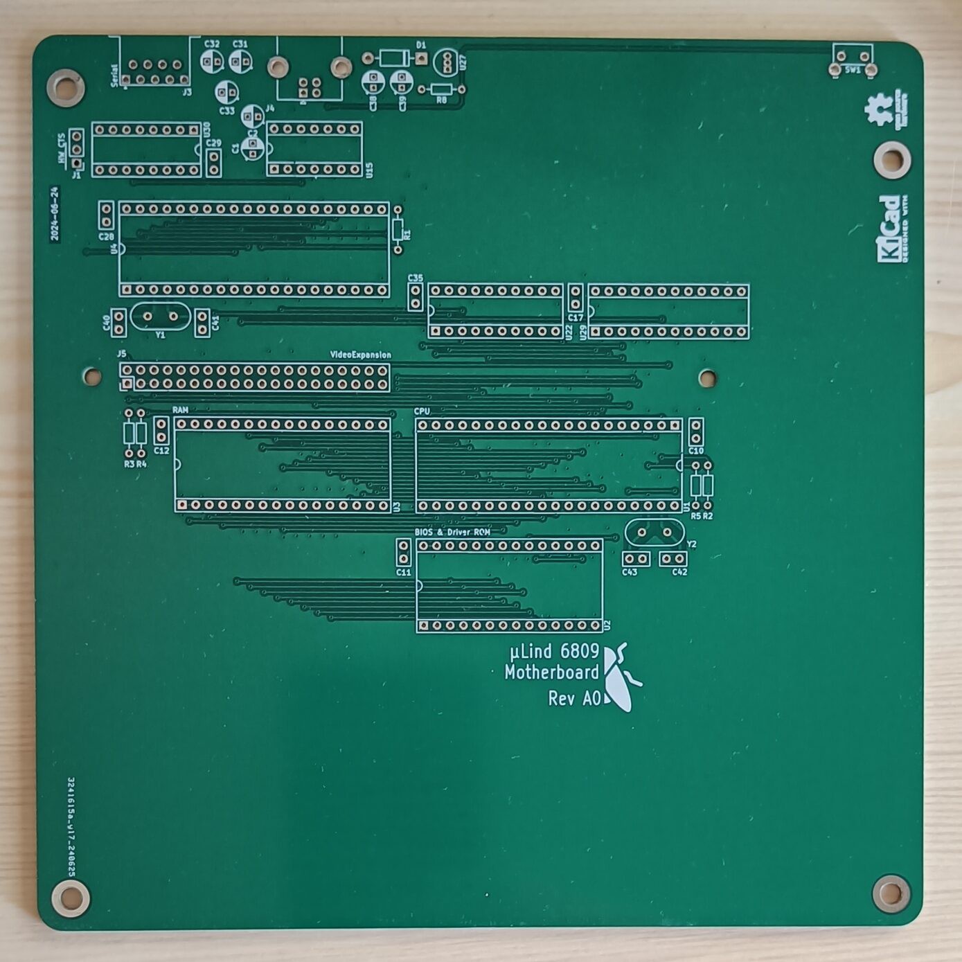
The stage 2 is based on stage 1, with some modifications, bug fixes (see table below) and addons according to the implementation table. The main goal of doing this in stages and keep formfactor between stages was to be able to make a case to place this board in, and this case would work for any board no matter what stage it was from. And I will also have the advantage of being more assured that the schematics is correct, at least the carry over parts. The picture below is the final layout of stage 2 , the one that was ordered.

Found bugs in stage 1, irq-proto and 6522-proto:
| Bug | Origin Component | Resolution |
| Missing pullup on nMRDY pin | CPU on stage 1 board | Added pullup in stage 2 |
| Lost terminal on reset, reset pin on USB interface connected to board reset. | MCP2221 - USB interface on stage 1 board | Added optional jumper to reset pin on MCP2221 |
| The computer would not work when parallel proto board was connected, enable signal connected to wrong CS pin on 6522. | 6522 parallel interface on 6522 proto board | Swapped CS0 and CS1 on stage 2 implementation of 6522 port. |
| Computer stopped working when irq proto board connected, Read signal to irq register inverted logic. | Register chip on irq proto board | Added NOR inverter to OE signal on register U21 on stage 2. |
| Irq register was never cleared after a triggered irq, register only latched on read signal. | Register chip on irq proto board | Used Q clock (rising 90 degrees before the read signal, ensures us that register is always updated. |
| Irq value put in register is wrong, irq bits routed in wrong order | NAND gates between priority encoders and register on irq proto board | Re-routed signals between NAND gates (U20) and register (U21) on stage 2. |
With all these bugs fixed we could order stage 2 with higher confidence.
Bugs found in stage 2, so far:
| Bug | Origin Component | Resolution |
| Missing pullups on bus signals outside the bus trancievers | Bus trancievers | Added in stage3. Will hopefully not cause problems in stage 2. |
| R/W signal to data bus tranciever was in wrong direction | Bus trancievers | Changed GAL logic on that pin. Will be direct from processor in stage 3. |
| Intensity for RGB led is wrong, shows almost only blue. | PWR_LED | Analyze what resistors it should be for the individual colors. |
| Footprint for power switch had to small pin holes | Power Switch | Updated footprint for stage 3. |
| Missing/wrong pins for power/gnd on serial controller. Bad footprint. | Serial Controller | Updated footprint for stage 3. |
| IRQ signals not in correct order | IRQ-Handler | Rename sipnals to reflect "lower number - higher priority" on stage 3. |
Stage 3 (status: DESIGNED and Updated from Stage 2):
For this stage the schematic is ready, and a preliminary routing has been done. I will update this during the testing of stage 2 for any problems or faults we will find during testing of both the prototype boards and the stage 2 board. But this stage will hopefully be the "final form" of this project, which means that I can focus on developing addon boards and expansion boards.
System In greater detail:
So... What is this then? Well... It is a fantasy coming true for me and my son at least. But more to the point I would hope that it will be an interesting platform for retro development, both for games and operating systems. Me myself have had a long standing dream of making a "multi-tasking" OS with process isolation for an 8-bit system.
So what is it then, for real?
Processor:
Since we based this system on stuff we were given from the beginning we settled for the MC6809 and in the long process of trying to make something of it we also found out that it had a younger sibling with a bit more energy, the HD6309. That processor looked even more interesting to play with.
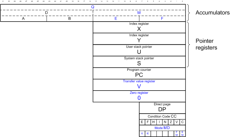
Image showing the register map for the 6309 with its 32-bit capable register. Source: Wikimedia
Memory:
I knew I wanted the possibility to store BIOS/Drivers/Monitor on a non-volatile storage so 8k of EEPROM seemed like a good thing to have. This might be revised if it looks like we need more. And for RAM I certainly knew that I wanted more than the measly 64k Offered by the regular 8-bit platforms. So I put 512kB on there and started thinking about some kind of memory management. The extra 512kB memory socket was introduced as a statement of overkill (Who does not "need" 1Mb of RAM!?!).
Memory Management:
As soon as I realised we wanted more than 64kB RAM I started looking in to a MMU, there are some commercial out there (The 74ls61x for example, an awesome explanation here). But most of them are either since long out of production or unnecessary complicated. So me and my son started brainstorm on how we could do it and we settled on a simple version where you use a 4x4 register chip (or 2 if a full byte extra address space is needed) and some additional logic to be able to read back what the register was set to (my son had some ideas in the operating system that needed to know).
Glue logic:
I started doing every logic step in discrete logic chips but it took too much space on a board that we actually changed most of them for a complex logic chip, a GAL. Or in our place we ended up with 3 of them. I also wanted to use them so I would be able to change the behaviour of control signals and address decoding later if needed.
Serial port:
In stage 1 I opted for a age typical 6552, a dual 6551. This was however a bit to slow (only 38600 baud) and lacking FIFO buffer, this was a recipe for slow application transfers when we started coding. So in stage 2 this is changed to a xr88c92/192, with 8 or 16 byte FIFO and possibility to run up to 230400 baud with the same crystal. The only downside is that I had to diverge from my goal to only use DIL sockets and accept a PLCC (at least the socket is still thru-hole). It is end-of-life but there is pretty good availability on them. During stage 1 we also found out that if we want the optimum transfer rates we need to use the CTS/RTS pins, which no DIL mounted USB interface chip had support for, so there will be a DIL14 sized board with a better serial-USB interface with support for CTS/RTS.
The parallel port:
We said from the beginning that we wanted C64 compatible joysticks. So a parallel port was added, a 6522 VIA. We chose that one since it is still quite available. The 6522 also brings 2 timers to the table which we really needed. One of them will be used as a 1kHz scheduler clock and the other will hopefully be used as a simple PC speaker tone generator for use in the BIOS.
IRQ handler:
I there will be an operating system we need interrupts! And the 6x09 only has NMI/FIRQ/IRQ. So we designed an interrupt handler that can handle 15 different prioritized interrupts and has the possibility to turn of some or all of them. It is however not able to handle multiple interrupts, just first come - first served.
PS2 interface:
I wanted to be able to use a keyboard and mouse on the system. Therefore it needed a PS2 interface, and just about that time Ben Eater uploaded some videos on how PS2 works (Ben Eater Youtube). This gave me the perfect opportunity to create a PS2 interface of my own.
Compact Flash interface:
After reading up on True IDE Mode on the CF cards I realized it would be quite simple to interface with those. I also found that RC2014 had some CF card adapters for their system and i looked at their schematics to see that it really was that simple (RC2014 CF adapter).