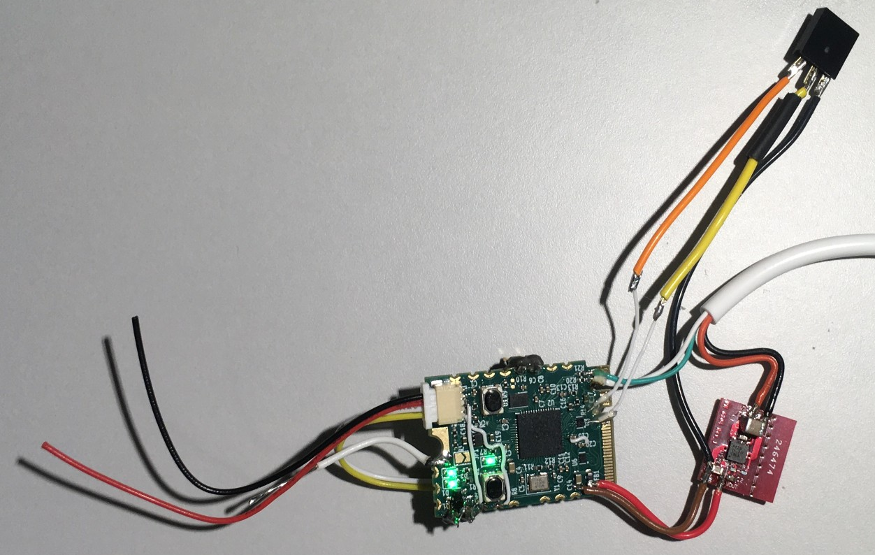
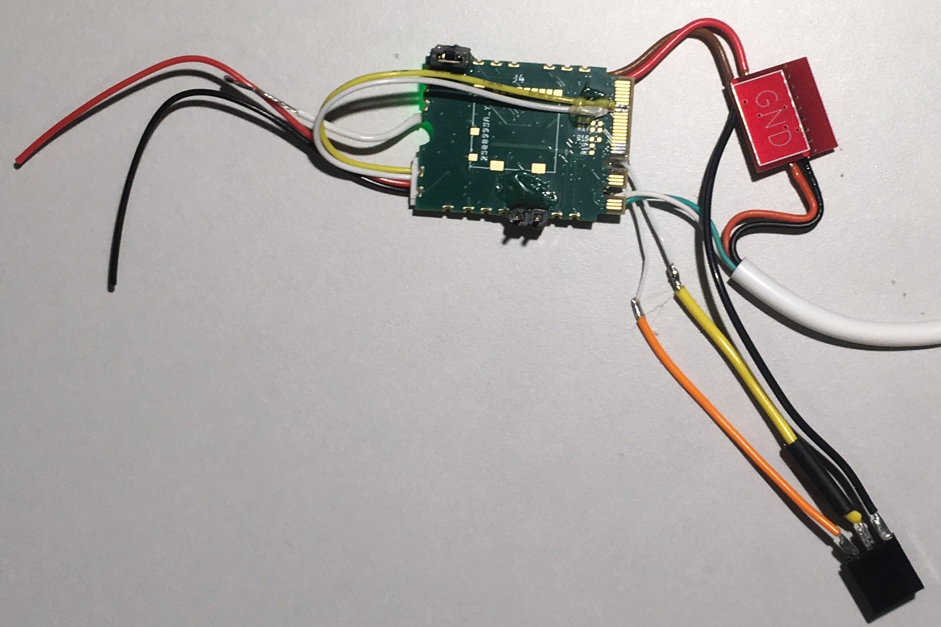
As it happens too often, this revision 1 board has its issues. With my RadXA ROCK 3A SBC not arrived yet, I was going for the fly-wire test approach.

 USB and power through an external 3.3 V regulator are working flawlessly. Power LEDs are on and the user LED is blinking away. Nice! UART on the m.2 and on GPIOs are doing simple loopback and the USB/UART is running a simple command line already.
Things that did not work out of the box: I2C (of course). I should pay more attention to the pin mapping. I cannot use I2C1 at the same time on the m.2 and the QWIIC connector. Also pin4 on the QWIIC is SCL, not SDA. Nothing a few cuts and wires cannot fix. Now I have a loop-back from the m.2 end to the QWIIC connector. One port is master, one is slave. Mint.
More wires will be required to test the uSD card, the SPI signals are connected up-sidedown to the SPI port on the RP2040. Pin mapping again! I blame this one on the schematic symbol, not showing all pin functions.
And the castellated holes will get their own log. Some cheap ideas are also bad.
 MagicWolfi
Discussions
Become a Hackaday.io Member
Create an account to leave a comment. Already have an account? Log In.