 MagicWolfi
Just received revision 2 of the board!
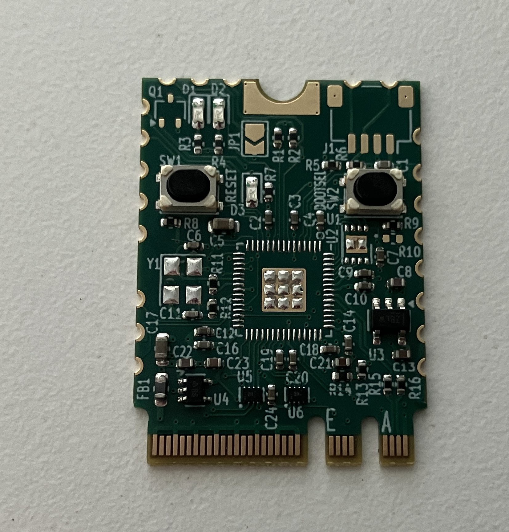
This time I went for real castellated holes on 3 sides, even though JLC charges an arm (pun intended) and a leg for it.
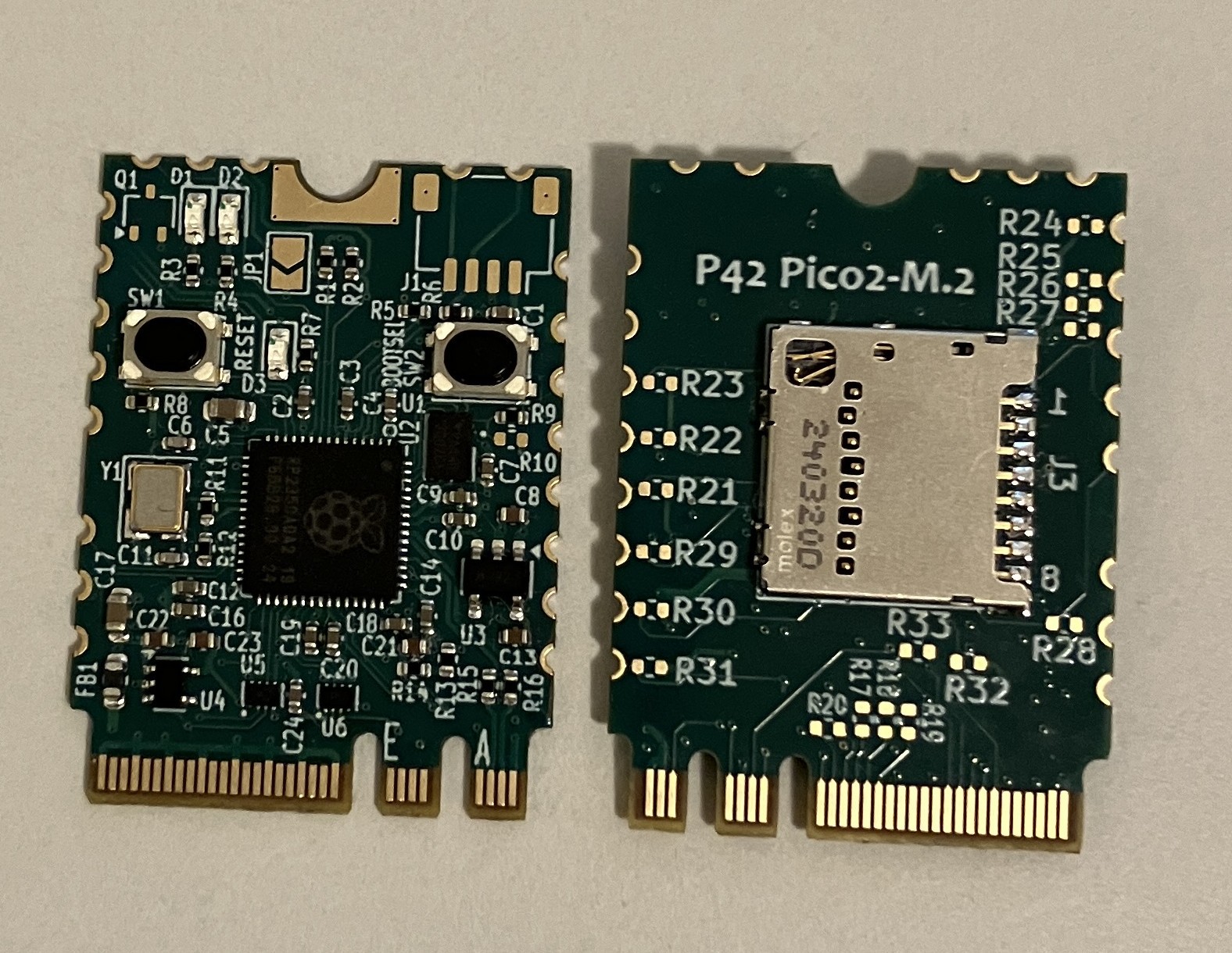
The 2nd big change is the switch to the RP2350, if you counted the pins. I was lucky to get into their samples program and have some RP2350A and B (including Flash and crystals) at my desk. Some soldering required.
Here is a nice view of the board and the castellated holes detail. Test firmware is running on a Pico2 already.
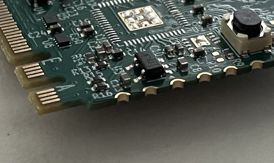
And some hot air soldering later, the board looks like this and is operational. SD card is alive, UART to the M.2 interface and all GPIOs. Still missing the QWIIC connector and a SC70 p-FET for the core voltage LED. Also the design decision to use an external LDO instead of the internal switcher for the 1.1 V core supply has proven to be good and will make the BOM cost being less.
Discussions
Become a Hackaday.io Member
Create an account to leave a comment. Already have an account? Log In.