The original haasoscope was great, and still is, but as time has passed (6 years!) there were many ways I thought of to improve it.
As I advanced in the kinds of projects I worked on, including high speed data acquisition for experiments at CERN, and one of the world's fastest random number generators, I found myself needing a much faster scope. I managed to get one, because I'm spoiled and have a great research budget, but I was shocked at how expensive they are. Even a probe was $1000+, at the low end!
I started investigating why this stuff was so pricey. What I found was
- The market for fast scopes is smaller, so companies need to charge more per unit in order to recoup their upfront R&D costs
- They charge more because they can! A lot of the high end scope market is made up of companies and institutions, for whom money at the $20-50k level is not an issue
I dreamed of one day making my own fast scope, to finally allow "ordinary people" to tinker with high speed electronics.
I was inspired earlier in 2024 by an open-source 2 GHz active scope probe on hackaday. I printed and assembled a few of my own, and they worked great, for under $100 each! The probe was already half the challenge (standard x10 passive probes are limited to under a few hundred MHz) - now I just needed a fast, affordable USB scope.
I did some research and initially hit some roadblocks. Most fast ADCs sent data out on high-speed serial links (12.5 Gbps+), which would require a "high-end" FPGA. Those can easily be many hundreds if not thousands of dollars, plus licensing fees for the software and IP, not to mention having to deal with assembling a 0.4mm pitch 782 pin BGA! I was entering a world of pain.
But I then found a TI chip, strangely affordable, that also had a parallel LVDS interface. I could then use a "low end" FPGA - there are plenty of them with 100+ LVDS pairs for under $100, and free software and no licensing. I still had to deal with a 256 pin 0.8mm pitch BGA and a 484 pin 1mm pitch BGA, and routing ~80 LVDS pairs, each running at 800+ Mbps, but it finally sounded doable in principle.
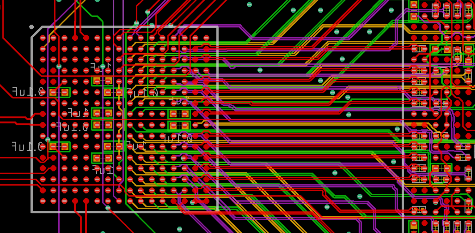
The routing was tough. At first I couldn't find a way to get all those signals out with less than 12 layers, and blind vias (as recommended in the data sheet / evaluation board layout). I priced it out and getting those made would be at least $500 /board in small quantities. (Blind vias are vias that connect only two specific layers of a multi-layer PCB, rather than holes going all the way through the board. They let you route other signals under (or over) the blind via, rather than having to go around it.) But I finally had a breakthrough and realized I could just get it to work, with only 10 layers, and no blind vias. I just needed thinner traces, 0.08mm (that's 80 microns wide!), and smaller vias, 0.2mm, directly under the BGA pads. Turns out that's just pushing the limits of some of the inexpensive Chinese PCB fabs, but they can do it! The boards can now be done for under $50 each in smallish quantities.

The last obstacle was dealing with those BGAs. The FPGA could be assembled overseas, but the ADC was not available in China. I priced out having a US assembler attach the BGA, and we were back close to $500 again. I wasn't going to pay that, especially for some prototypes, of which I'd likely need many iterations. Wait, could I assemble it myself?! I bought a reflow oven on Amazon for $300 and watched some YouTube videos. It didn't look that hard. After practicing with some cheaper chips, I finally tried attaching the ADC to my board. It worked! And the Haasoscope Pro was born.
 haas
haas
Discussions
Become a Hackaday.io Member
Create an account to leave a comment. Already have an account? Log In.