In July 2024, the kids were off to camp, and I was off from teaching for the summer. Relax? Vacation? No! Work day and night developing my own 2 GHz oscilloscope!
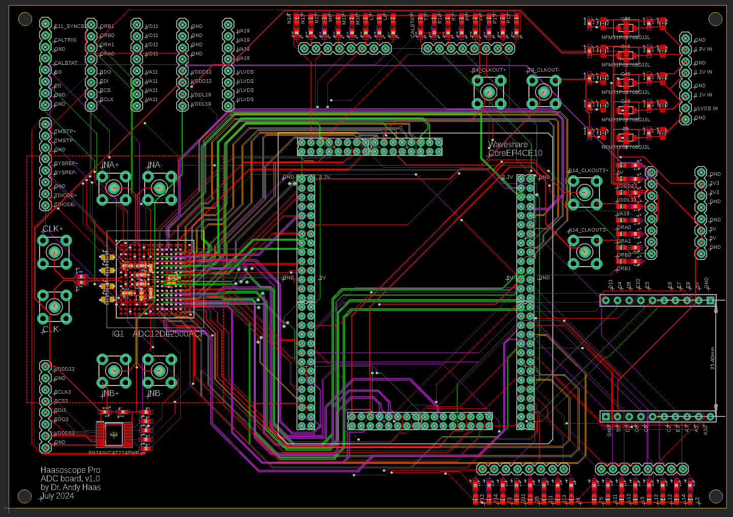
The first goal was just to talk to the ADC chip and get it to do something. This would convince me I could solder the BGA chip correctly in my little reflow oven reliably, power the chip correctly, and let me start playing around with it. I had to connect an FPGA to it, to talk to it over SPI and receive the LVDS signals it sends out containing the ADC data. So I wired it up to an FPGA dev board that I had experience using, based on a Cyclone IV FPGA. You can see in the pic below all the 2mm spaced pins where the dev board would connect to this new board hosting the ADC chip on the left. There were also SMA inputs for the (differential) clock signal and two analog input channels to the ADC. I also added lots of debug headers so I could probe every signal going into and out of the ADC, plus debug the power and signals from the FPGA. There's also two headers on the right for connecting a module based on the FTDI FT232H chip I had experience with for interfacing the FPGA to USB2.
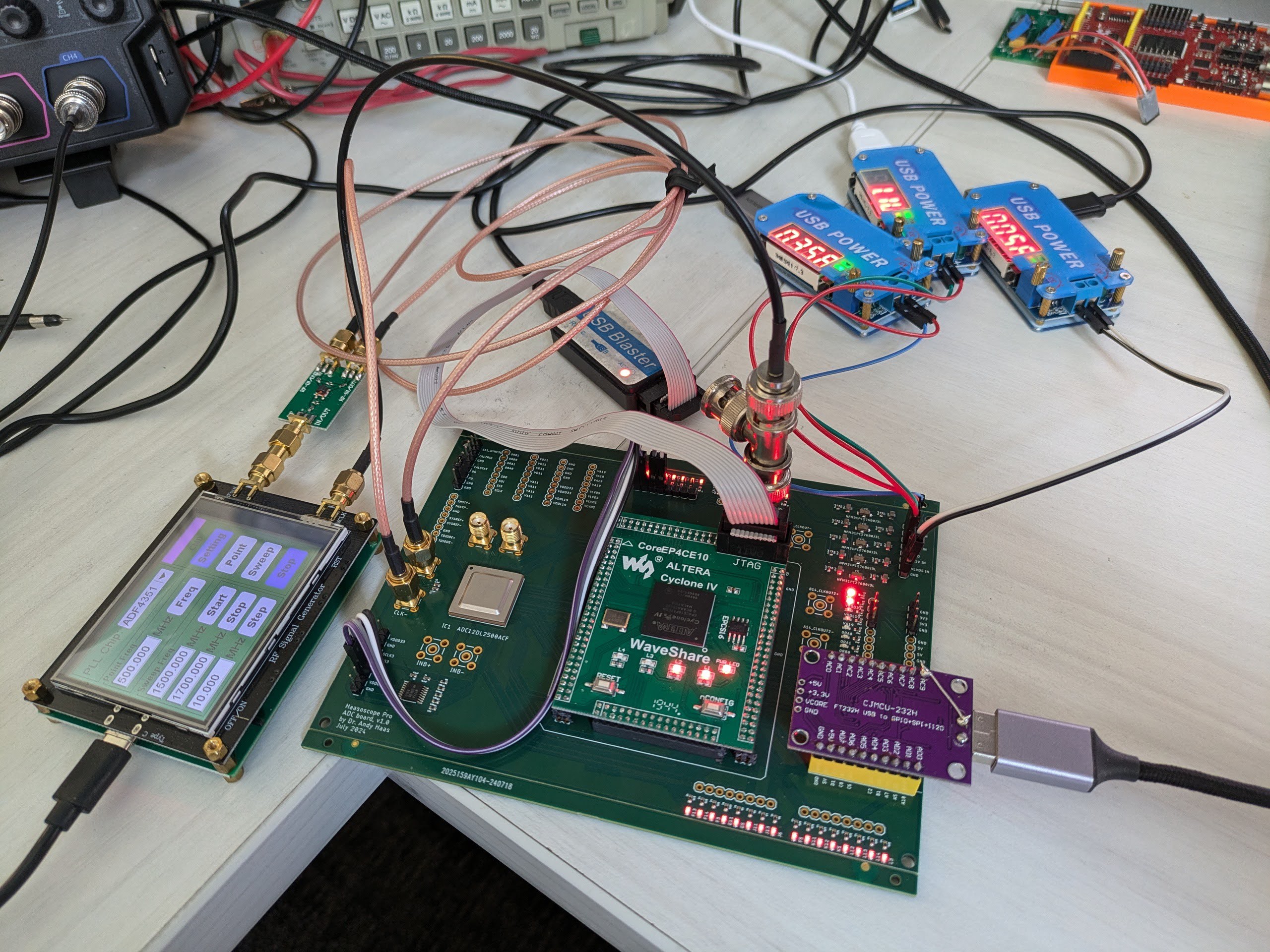
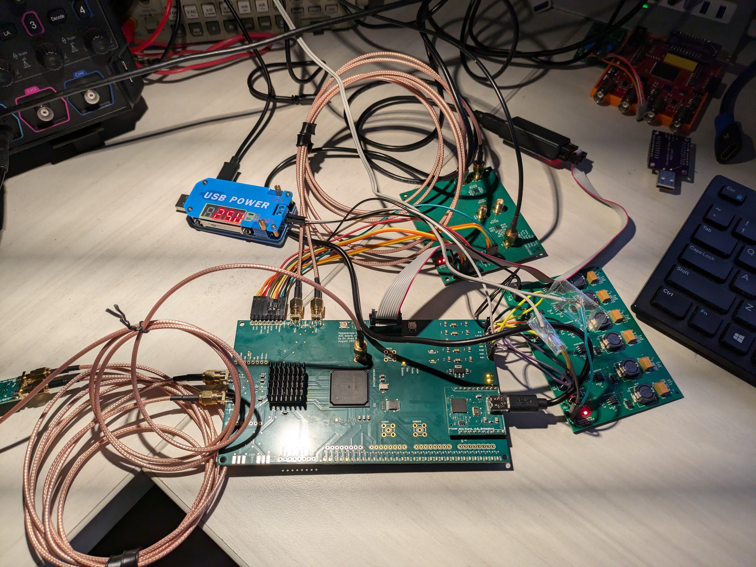
This is what the board looked like assembled, with everything attached to it. For power I was using these handy little USB-powered power supplies I found on Amazon to supply the ADC with 1.1V, 1.9V, and another 1.9V (separate for LVDS). The ADC also needs a very fast clock to tell it when to sample, 1.6 GHz. For this I used a cheap ADF4350 board from Amazon. But annoyingly it only had single-ended SMA output, whereas the ADC needed a differential output to two SMAs, so I used a cheap eBay single ended to differential converter. I also used another of these (not shown in pic) to input signals to the differential analog inputs of the ADC from my single-ended signal generator. To sync the clock between the FPGA and the ADF4350 board, I output a 50 MHz clock from the FPGA (big BNC connector sticking up) and connected it over to the reference clock input of the ADF4350 board.
A lot of things worked! I could talk to the ADC chip over SPI just fine, reading back it's Vendor ID and serial number, setting its registers, and power it up and down. It could also see the clock from the ADF4350, and I'd see data coming over the LVDS lines into the FPGA. Below you can see the binary LVDS data coming in, when I'm sending in a 10 MHz or so pulse to the ADC analog input - I do see the bits going from 0 to 1 in unison on most of the LVDS outputs! It didn't work fast, only up to about 200 MHz, because those LVDS lines were hideous - very different lengths, going through tons of vias and even 2mm pin headers and who knows what on the dev board, and even unterminated. But it was more than enough to encourage me to move forward with the project.

The next major step was clearly to put the ADC and the FPGA on the same board, and do the LVDS connections properly.
A very important lesson I'd learned, the hard way, was to break large projects into as many small blocks as possible. Especially for large hardware projects like this one, you don't want to put everything on one board at first. Start with each block on its own little board. Then it's quick, easy, and cheap to iterate versions of each little board you're working on, without redoing the other boards that already work fine.
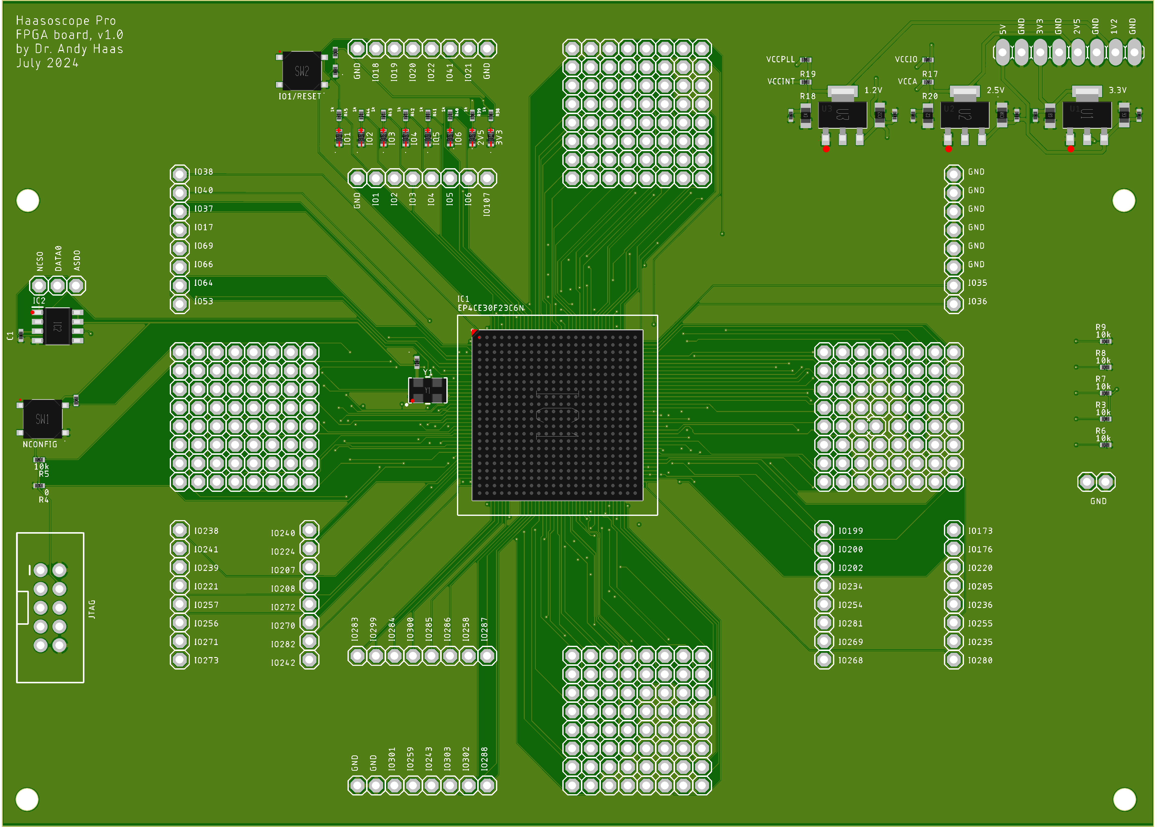
So I first made just a board with the FPGA on it, to get that working on its own. You can see a render of it below. It didn't really do anything except prove I could power it, program it with firmware over JTAG, see a 50 MHz clock input from the crystal, and make some LEDs blink. I also fanned out to .1" headers all the IO's, in case that would even be useful to me or others.
The board worked just fine, first try!
So then I was ready to make a board with an ADC and an FPGA on it, basically by merging together the first ADC board and the new FPGA board.
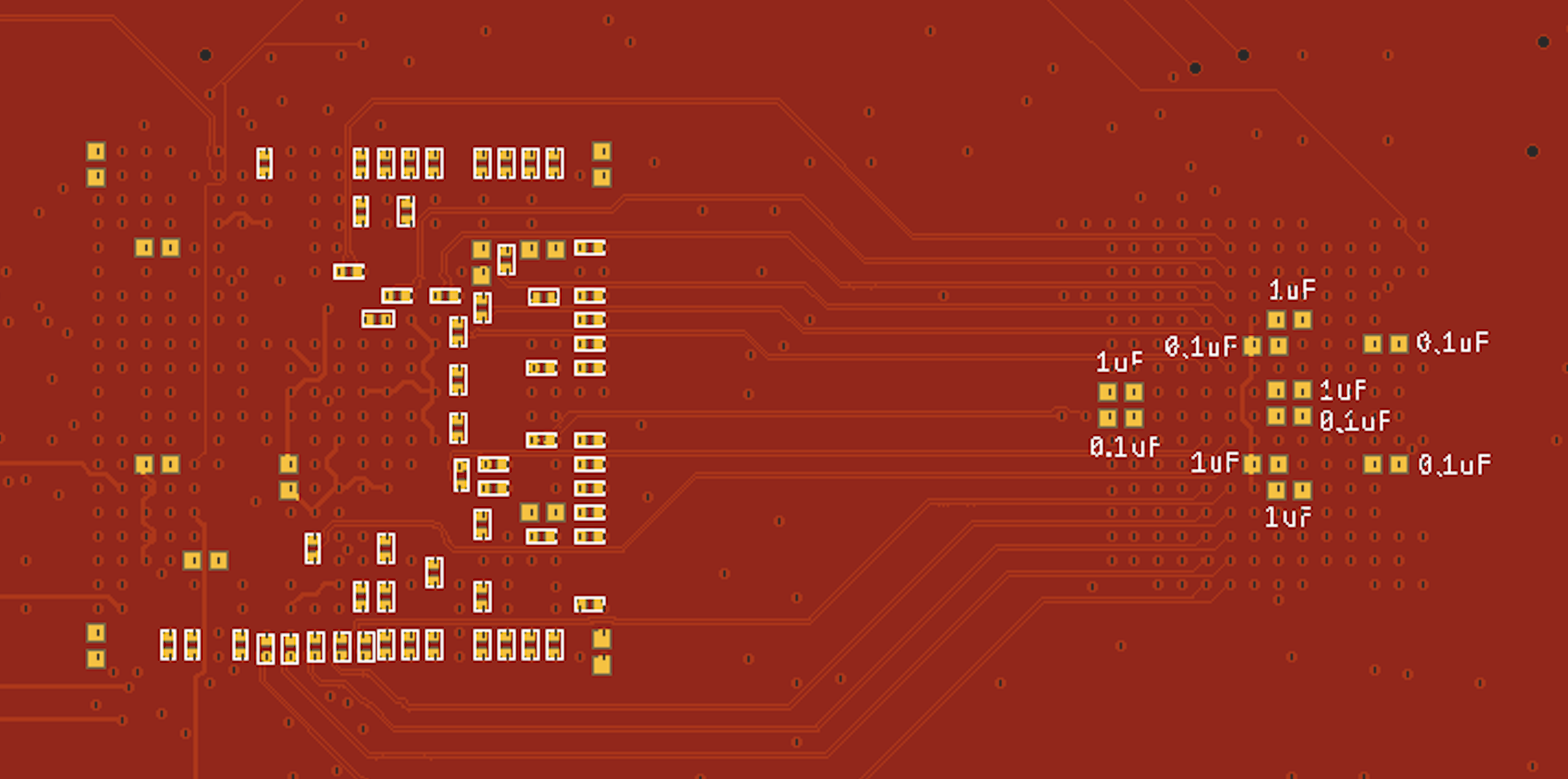
The LVDS signals from the ADC to the FPGA needed to have 100 Ohm termination resistors at the receiving FPGA side. That's 56 termination resistors, and they have to all be close to the FPGA. Some FPGAs have built in resistors for this purpose you can enable in firmware, called on-chip-termination (OCT). But the Cyclone IV chip I wanted to use didn't have that feature, nor the Cyclone 10, just the pricier Cyclone V. Fortunately, it turned out it was easy to add these resistors physically on the board. They just had to be 0201 size, and on the bottom of the board, directly under the FPGA, where each LVDS line came to two vias to get up into FPGA, as seen in the pic of the bottom of the board below. (The FPGA is on the left, and the ADC is on the right. You can also see the decoupling caps for both chips there.) But surely this would cost a lot extra, no? I'd now need two-sided assembly, top and bottom, and down to a 0201 package, not just 0402. Nope - JLCPCB gives free two-sided assembly and down to 0201 by default for all boards with 6+ layers!
You can see below what the "ADC FPGA board" looked like in real life, with everything hooked up to it. There's now also a "power board" to provide the ADC and other things with all the voltages they need (on the right), an "input board" (on the top) to do the single-ended to differential conversion plus amplification of the analog inputs to the ADC, and a "data board" to replace the purple Amazon FT232H board that talks over USB2 to the FPGA. I still have one Amazon power supply for the FPGA since I forgot to make 2.5V on the power board initially. The clock is still supplied by the ADF4350 board the same as before.
Even more things were working well here, as you can see below. I may have shouted out some expletives and then cried a little when I finally saw a sine wave on the screen from the Haasoscope Pro for the first time. :)

Next piece to tackle was the "clock board", to replace the ADF4350 board from Amazon. That turned out to be simple - I just copied the reference ADF4350 design (basically the same as the Amazon board, but without the screen etc.) and put it on my own board. You can see it on the bottom in the pic below. Things are starting to look a bit more neat and tidy! I also added some DC offset circuitry to the input board using a dual 16-bit DAC.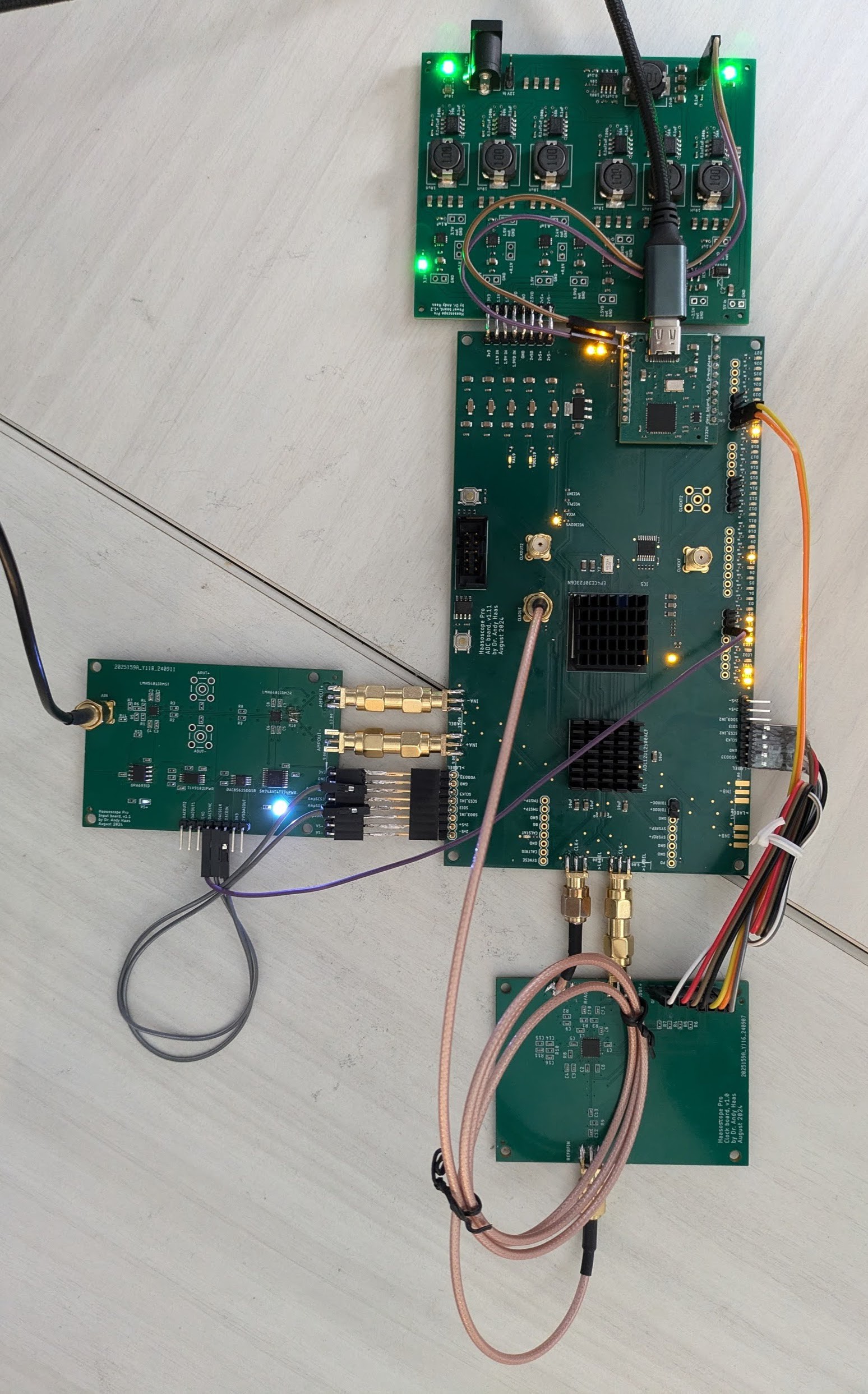
The last board I worked on was the pre-input board, that handles annoying analog stuff... 50/1M switching, AC/DC switching, attenuation, etc. You can see a render of it below, with 3 relays and some carefully calculated 50 Ohm traces. It mostly worked fine too, though I had to mess around with different relays, connectors, and photo mosfets to maintain the 2 GHz of bandwidth. I even had to buy a cheap but wonderful NanoVNA V2 PLUS4 vector network analyzer to debug it all!

By the way, all these individual test boards are still available in the GitHub in the "sub boards" directory.
The last step was just to combine all the test boards together onto one board, and we had the first full prototype of the Haasoscope Pro!
 haas
haas
Discussions
Become a Hackaday.io Member
Create an account to leave a comment. Already have an account? Log In.