When you hear "2 GHz oscilloscope", you might rightly wonder what kind of analog wizardry can possibly achieve such crazy bandwidth. Well, as you'll see, there was some care involved, but the real key was just to use some incredible components. In particular, the LMH5401 is a preamplifier with 8 GHz of gain bandwidth product that somehow only costs ~$10. We use it as a 4x gain, single-ended to differential amplifier. Then following that is the LMH6401, a 4.5 GHz bandwidth variable gain amplifier that somehow only costs ~$15. We use it to vary the gain by an extra factor of between -6 to 26 dB (~0.5x to ~20x), in 32 steps. Just using those two components, we basically have a 2 GHz front-end. The rest is just bells and whistles.
The front-end is basically all 50 Ohm (or 100 Ohm differential) impedance. 1M Ohm input impedance is accepted, but, as you'll see below, it is immediately turned into a 50 Ohm signal and then handled just like a 50 Ohm input.
Let's take a look at the schematics. The first page is the "pre-input" part. A single-ended BNC signal comes in, and a 50 Ohm single-ended signal comes out, which will go to the LMH5401 preamplifier on the next page. Along the way, we are handling the splitting out of an analog input for oversampling, switchable 50/1M Ohm impedance, switchable 5x attenuation to increase the dynamic range, and AC/DC input coupling. The main goal here is to accomplish these functions without ruining the 2 GHz bandwidth before we get to the fancy preamplifier on the next page.

We do have to be careful about the BNC input itself. Connectors are easy places to destroy bandwidth. Some BNC connectors only have 500 MHz or 1 GHz of bandwidth! We use Molex 73100-0105 BNC connectors, rated to 2 GHz, but I've tested them to 3 GHz and they show minimal losses (<1 dB).
Next is a stage which can optionally split out half the signal to an SMA output on the front, so you can send it to a second Haasoscope Pro for oversampling. This is only on channel 1, since if you're bothering to oversample the signal, you're going to be using the ADC in single channel mode to first get the full 3.2 GS/s for the channel. The splitting is done by a simple resistive divider in the Delta configuration. It maintains the 50 Ohm impedance of the signal along both paths. We're assuming that the signal is 50 Ohm here, because only 50 Ohm has 2 GHz bandwidth and would require oversampling. Half of the signal is lost to heat, but that's OK, we have amplifiers afterwards.
This, and other options, are switched on or off by a relay. But not just any relay - most will only have a few hundred MHz of bandwidth. We need special "RF relays". Here I settled on the Omron G6K-2F-RF-T, which is rated to 3 GHz, but really starts to degrade significantly after 2 GHz. But that's good enough for us here, and already it's ~$10 each. Better relays are available, but can easily be ~$100 each! They're DPDT relays, so it's easy to route signals either on one path or another path, since there's an "input" and an "output" switched simultaneously. If the relay is off, the signal just goes straight through on a 50 Ohm wire to the output. If the relay is on, the signal goes into the splitter and half of it goes to the output.
The next stage allows for switching to accepting 1M Ohm input impedance, for using standard 10x passive probes. These probes inherently don't have large bandwidth - the ones I usually use, the Rigol PVP2350 have 350 MHz of bandwidth, and the most you're likely to get from any passive probe is about 500 MHz. This is far from 2 GHz, so why bother with 1M Ohm impedance at all? Well, for one, some people just like to use 10x passive probes and don't care about the bandwidth. Second, if we're in two channel mode for the ADC, we have 1.6 GS/s per channel, and that's not such overkill for 500 or even 350 MHz of bandwidth.
The goal here is to deal with 1M Ohm input impedance, but then immediately turn it into a 50 Ohm signal, for processing like a 50 Ohm input. This lets us reuse the same magical high bandwidth 50 Ohm amplifiers we use for a 50 Ohm input. We "only" need to maintain ~500 MHz of bandwidth here, since the passive probes won't have more than that anyway. Here we make use of another fantastic chip, the OPA859 op-amp, with up to 1.8 GHz of bandwidth, somehow for only ~$3. At 2 Vpp, the bandwidth is down to 400 MHz, but that's still pretty much good enough. And importantly, the inputs are CMOS MOSFET inputs, meaning they are crazy high impedance, like 1G Ohm, with just 10 pA of input bias current. That means we can put a 1M Ohm input into it, and not have the amplifier itself affect the input signal.
A 1M Ohm input resistor from signal to GND sets the input impedance. We also want the input capacitance to be ~10-15 pF, which is what is expected by passive probes and standard for oscilloscope 1M Ohm inputs. The tuning screw on the probe can adjust the compensation, within a range, to account for varying oscilloscope input capacitance. I've found that the parasitic capacitance of the Haasoscope Pro input path, from the BNC input connector, the board traces, the component pads, the buffer amp, etc. seems to be about 10 pF already, so although the pads for an extra capacitor are there on the board, I don't add one at the moment. We use the op-amp as a simple unity-gain non-inverting buffer, and a 47 Ohm resistor is put on the output to make the total output impedance close to 50 Ohm.
The following stage is the switchable 5x attenuator, for increasing the dynamic range. It is 50 Ohm impedance, since everything is 50 Ohms at this point. It's a simple resistive pi-attenuator. This nifty calculator can tell you the two resistor values to use to get the desired attenuation while maintaining 50 Ohm impedance.
The final stage is AC/DC switching, which we do basically like all oscilloscopes do. A capacitor does the DC blocking, letting through only signals less than 1/2piRC. For us, R is 50 Ohm, so C needs to be as big as possible - we use 1 uF, giving a ~3 kHz cutoff. DC signals are let through by a photo-MOSFET when it is on. We need to make sure it doesn't add capacitance and ruin bandwidth though, so the TLP3475 is used. We could have used another relay here, but the photo-MOSFET is only $3, vs $10 for the relay, and there's two channels, so $14/board saved, plus less signal degradation and less board space. We also need to make sure the capacitor doesn't add significant impedance, something we don't usually worry about - but at some large frequency every capacitor becomes an inductor, past its "self-resonant" frequency. Fortunately, Samsung provides data on their capacitors, and for the one we use, it is indeed an inductor at 2 GHz (with a self-resonant frequency around 10 MHz!), but its impedance is only ~1.5 Ohm at 2 GHz, so not significant compared to 50 Ohm.
The second page is the "input" part. It takes in the 50 Ohm single-ended signal from the pre-input stage and puts out a 100 Ohm differential signal for the ADC. We already talked about the magic of these two parts, the LMH5401 and LMH6401 at the beginning of the post. Just follow the datasheets and they work. One detail is that I'm still optimizing the "termination resistor", the 357 Ohm one on OUTPATHMAIN. It sets the overall input impedance of the amplifier, and it seems like it's not quite 50 Ohms at the moment with 357 Ohm, despite saying it should be in the datasheet. Maybe my parasitic capacitances and/or inductances are a bit different than on their evaluation board? I'm working now on tuning it.

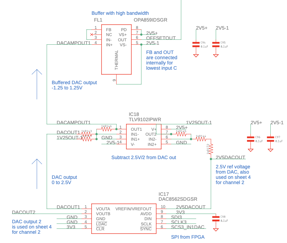
Along the way, we also apply an analog DC offset to the input signal. It goes to the "positive" input of the LMH5401 preamplifier. A dual output 16-bit DAC provides the settable offset voltage, which then goes through a low-bandwidth jelly-bean op-amp to move it from 0-2.5 V to -1.25 to 1.25V, as well as buffer the output. Then that output is fed to another OPA859 high-bandwidth op-amp, since we need to provide constant, low, output impedance to the LMH5401 input from DC - 2 GHz. (Reduce BOM count wherever possible!)

That is all for the first of the two input channels. Pages 3 and 4 just repeat this for for the second channel, except that the analog splitting is only done for the first channel.
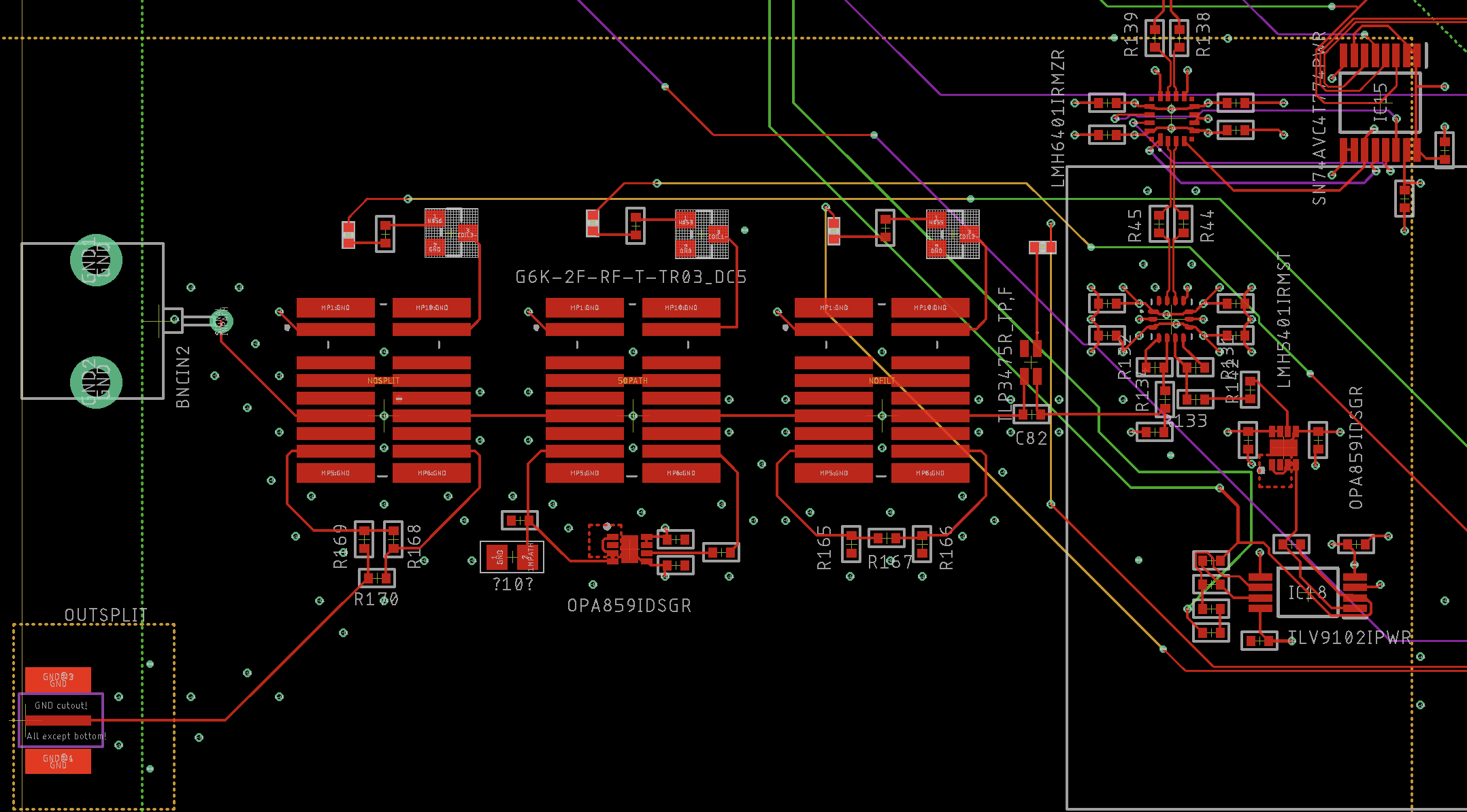
You can see the routing here, for the first channel. Starting from the BNC, all traces are 50 Ohm impedance, which means keeping them on the top of the board, layer 1 (red), and 0.16mm wide, given the 10 layer board stackup being used, with GND on layer 2 (not shown). There's also copious GND vias around the traces, at least every 1/10th of a wavelength at 2 GHz, which is about 30 cm * GHz (speed of light) / 2 GHz / 2 (sqrt of dielectric) / 10 = ~1 cm. And there's GND fill on the top layer (not shown), with 0.15mm between the GND fill and the traces, so nice coplanar waveguides.

And that's all there is to a 2 GHz front-end these days!
 haas
haas
Discussions
Become a Hackaday.io Member
Create an account to leave a comment. Already have an account? Log In.