The Haasoscope Pro can be used in several configurations, leading to three different per-channel sample rates:
- One device with both channels active, so 1.6 GS/s on each channel
- One device with just one channel active, so 3.2 GS/s on one channel
- Two devices with just one channel active total (oversampling), so 6.4 GS/s on one channel
(You also could have two devices with one channel active on each, or two devices with two channels active on each, or two devices with one channel active on one and two channels active on the other, or more than two devices with all sorts of combinations! But any channel will still be at one of the three sample rates mentioned above.)
However, the analog bandwidth of each channel will still be at least 2 GHz in all these cases. In fact, it's only down by ~-3 dB by 2.5 GHz, and significant signal ~-10 dB still gets through by 3.5 GHz. This leads to a problem called aliasing, whenever there is analog signal coming in with a frequency greater than half of the sampling rate. For instance, even for the highest sampling rate, 6.4 GS/s, we would ideally have no frequencies entering the ADC above 3.2 GHz. But unless we do something, the signal is only down by ~-6 dB at 3.2 GHz. And things would be much worse even for the lower sampling rates.
The effect is that those higher frequencies would look like lower frequencies in the ADC output, e.g. a sine wave with a frequency of 3.3 GHz would look like a 0.1 GHz (100 MHz) sine wave when sampled at 6.4 GS/s. That is inaccurate and confusing! Here's an example of an 800 kHz wave being sampled at 1000 kHz, and the result looking like 200 kHz.
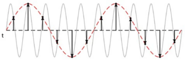
To combat this issue, we need a low-pass filter in front of the ADC to filter out higher frequencies. In fact, we'll need 3 different filters with different cutoff frequencies (0.8, 1.6, 3.2 GHz) to address the 3 different possible sampling rates we can have (1.6, 3.2, 6.4 GS/s). There are all sorts of filter designs out there with various pluses and minuses. Some filter types are really flat in the passband, but then suffer from a slower rolloff after the cutoff frequency, or vice versa. There's no perfect filter - you have to just pick the design that has properties which suit your application. I'm pretty sure you can spend a full year in graduate EE school just studying filter design!
I chose the 6th order Modified Chebyshev filter with 0.5 dB ripple, because it has pretty fast rolloff and is pretty flat in the passband. Thanks to a plethora of free online design tools, designing the filter is trivial. Due to limited rolloff rate, we can't set the cutoff frequency to 3.2 GHz if we want strong suppression beyond 3.2 GHz. Setting the cutoff frequency a bit lower, like 2.8 GHz, gives the filter time to roll off. This is what the calculator gives:
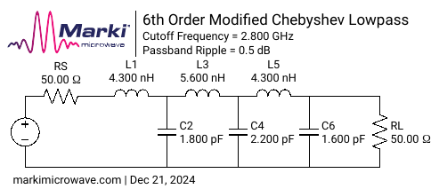
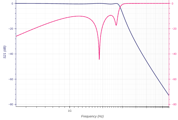
As you can see, the response is down ~-12 dB (a factor of 4) by 3.2 GHz, and is really flat until ~2.7 GHz. You could try a higher order filter, with more components, to get a faster rolloff, but then you also get a larger delay of the signal near the cutoff. This 6th order one has just ~100 fs of delay below ~2.3 GHz, which is OK for the targeted ~175 fs risetime of our 2 GHz system.
Well, that's the theory at least. Of course reality is a bit trickier, especially when dealing with single digits of nH's and pF's. Recall that a 1 mm trace has an inductance of ~1 nH, and an 0805 set of pads has close to ~1 pF of capacitance with a nearby ground plane - so parasitics are going to be significant here! This is what my little test circuit looks like:
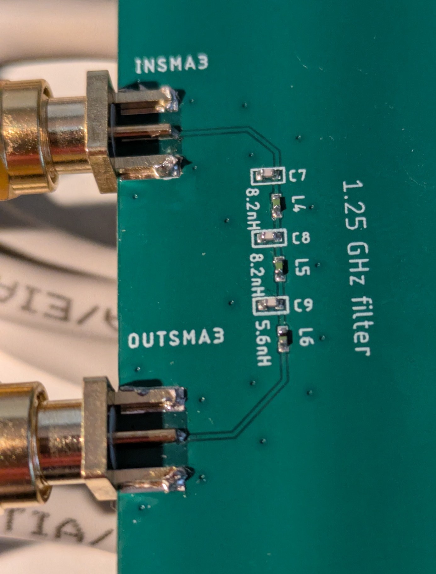
And here's how that board with a 2.5 GHz theoretical filter actually performs, as measured with the Nano VNA:
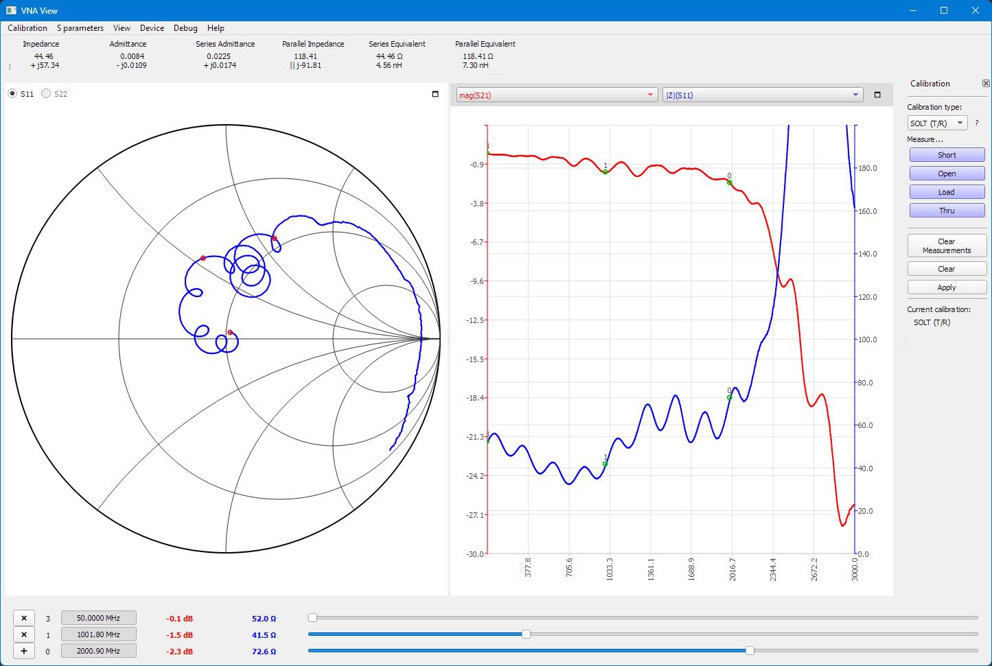
It starts to rolloff about 500 MHz low, so around 2 GHz, but it does have just ~0.5 dB of ripple in the passband, and it does rolloff at the right rate. We need a little tuning of the inductances and capacitances, to account for the parasitics. Here's what it looks like with 3.9, 5.1, 3.9 nH, and 1.2, 1.5, 1.0 pF (i.e. about 0.4 nH and 0.6 pf less per component):
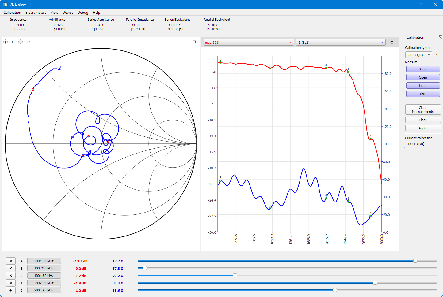
That looks pretty good! It's flat up to ~2.4 GHz and then drops off nicely. Hopefully it'll still work well on the real board, since the parasitic capacitance will be a bit higher on the 10-layer Haasoscope Pro board with a GND plane just 0.1 mm away, rather than 0.2 mm away like on this 4-layer test board.
 haas
haas
Discussions
Become a Hackaday.io Member
Create an account to leave a comment. Already have an account? Log In.