Before starting this project, I was familiar with logic gates and full adders and had modeled them in software, but I had never attempted to build one in hardware. I chose to use Resistor-Transitor Logic because it seemed the easiest of the logic families to construct from discrete components.
I first modeled the circuit in LTSpice using the commonly shown XOR, AND, and OR gates for the circuit. I designed the XOR gate using AND, OR, and NOT gates as well.
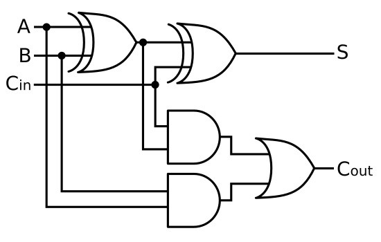
However I learned that combining AND and OR gates in resistor-transistor logic does not work well because these gates place the transistor in an emmitter follower configuration which causes a voltage drop on the output signal. Chaining multiple gates in this fashion causes unreliable behavior. After a quite long detour into learning about transistors and saturation, I realized I could use NOR gates to construct the circuit.
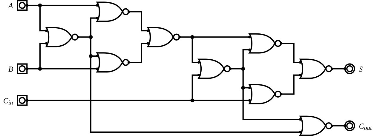
NOR (and NAND) gates are a universal gate and in RTL, the NOR gate uses the common emitter configuration which puts the transistor into saturation and does not cause any loss of voltage in the output signal. I chose to use NOR gates instead of NAND gates because they minimized the number of transistors I needed to use and reduced the board space requirements.
Here is the RTL NOR gate schematic.
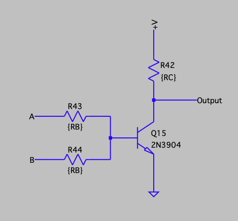
For the resistor values I choose to use
- RB = 10k ohm
- RC = 4.6k ohm
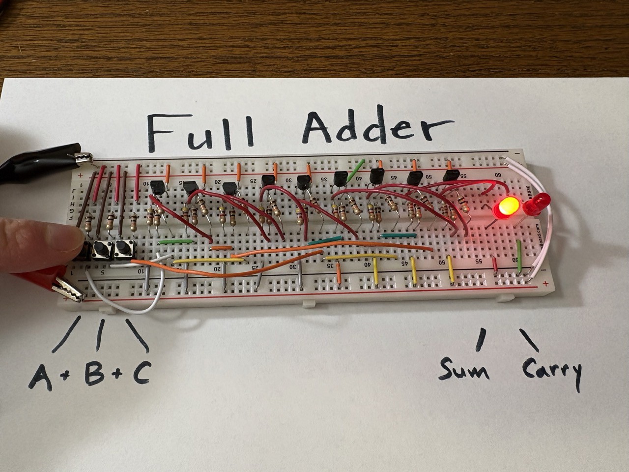
I first modeled the adder circuit in LTSpice and then built this single bit prototype on a breadboard.
From here I started building this circuit on perfboard. I iterated over many layouts but ultimately decided to leave the transistor layout the same as on the breadboard. It made copying the circuit over simple and I thought it has an intentional, artistic look to it. Each board contains two adders mirrored across the long axis. There is a positive rail down the middle and ground rails on the outside edges. The board was not wide enough to run all connections on the front side so I used insulated jumper wire to create some of the cross connections on the back side.
This schematic provides an approximation of the circuit layout on half of the board. From each transistor, the longest wire connected to the positive rail provides the output signal and the two shorter leads from the base are the inputs.

Using insulated wire for the cross connections proved a bit tricky because it easily melted if it was in contact with another lead which was then soldered. I learned to use the continuity testing mode on my multi-meter to debug unintentional connections through melted insulation. My soldering was also a bit messy and I found one very fine solder bridge between two leads. I tried to layout components so each solder point had a gap around it, but it wasn't possible in all cases.
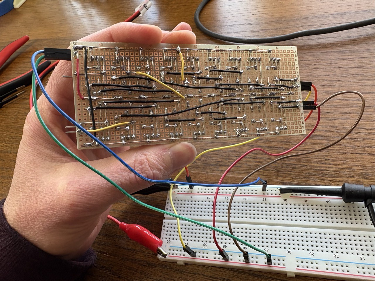
Throughout the construction, I used yellow wires to indicate carry signals.
The second board was nearly a copy of the first one so was much faster to construct except for debugging melted insulation on one wire which was difficult to locate.
For setting inputs I chose to use some inexpensive SPDT switches with a strong clicking action. I was hesitant to solder the leads since reviews said the plastic case easily melted so I ran wire through the holes on the leads and wrapped it once or twice before crimping the connection. I continuity tested every switch successfully. So far the connections have held.
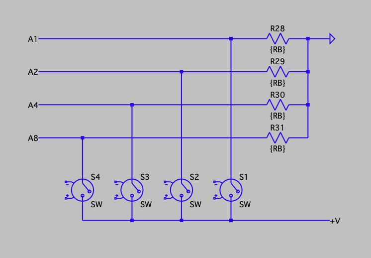
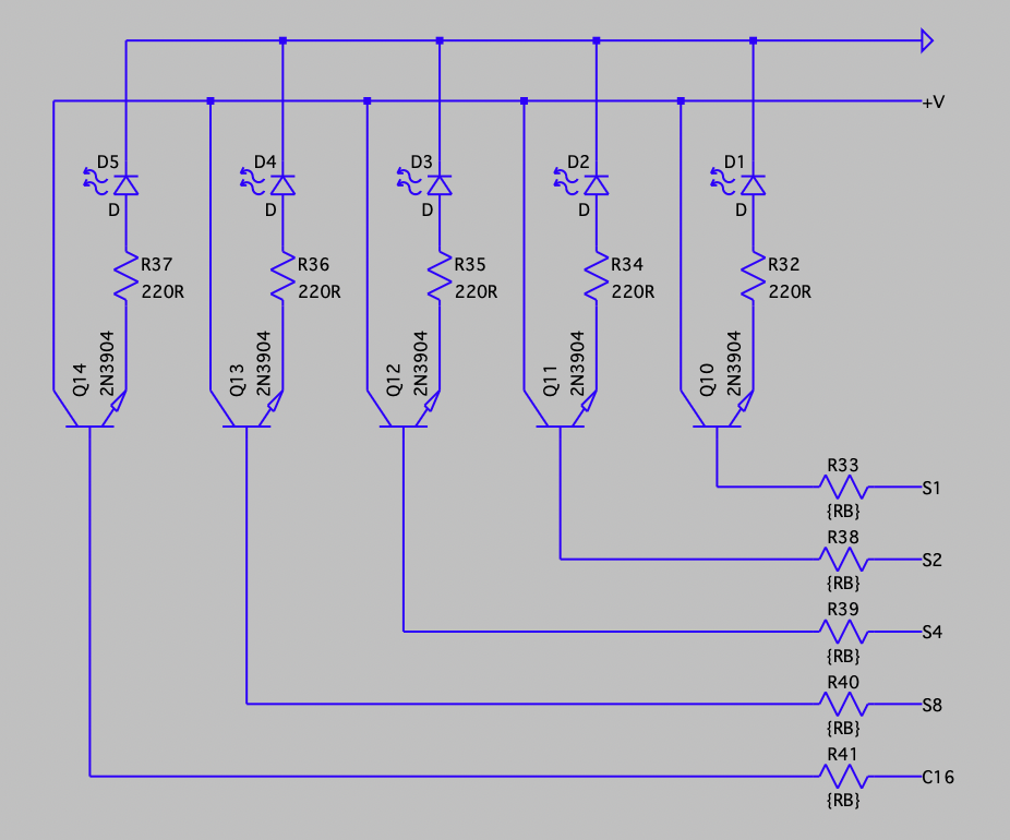
I constructed a third board for the input and result logic. The schematics of this board are below.
I mounted the boards and switches on plexiglass so I could show off the reverse side of the boards since that is the most impressive part of the construction in my opinion. I used standoffs, but had not considered mounting holes when building the boards so it was a bit tricky to mount them. I drilled too close to solder connections and had to resolder a few places. I also did not have the proper drill bit for plexiglass so I used a wood bit which caused the glass to fracture...
Read more » Ryan
Ryan


Great project, I bet you learnt heaps while researching and building this. Keep it up. Reminds me of Usagi electric UE1 vacuum tube 1 bit computer I see on youtube. Check it out