 Julius
Creating the Schematic
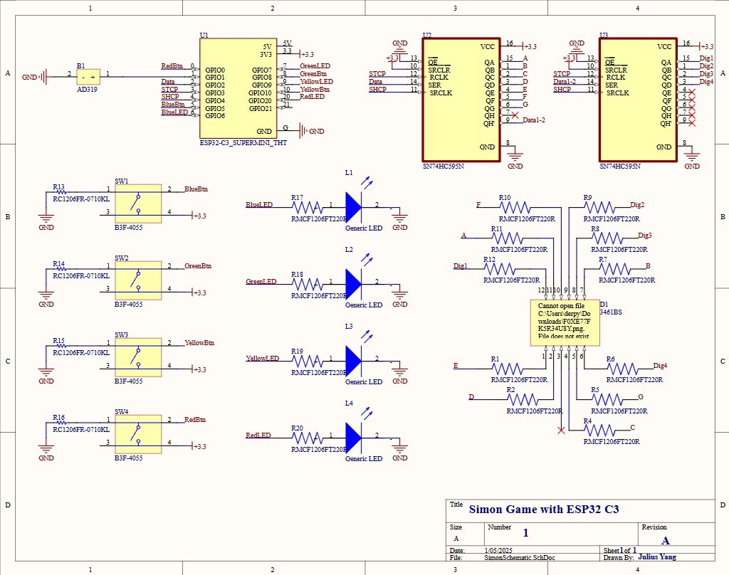
After prototyping everything on Wokwi and confirming it with a simple test circuit I moved on to create a schematic of the circuit in Altium Designer. First was to find footprints to represent all of the components I have in the circuit. For some, like the 74hc595 shift register I was using, it was very easy to find symbols, footprints, and their corresponding 3D model. However, for other components I could not find any of this information, so I had to create my own components using the dimensions from their datasheets. After creating the components, I wired them up on the schematic, double-checking to ensure that I did not miss a component and did not mess up on the wiring. This is the final result of that schematic:
PCB Design
After wiring my components on the schematic, it was time to turn that design into a PCB! Altium associates all of the schematic symbols with their PCB footprint, so when transitioning to part placement all of their footprints, along with their nets transferred over.
An important part of my design was that I wanted the PCB to be easy to hold, and easy for the player to use. Since the game requires the player to constantly press buttons, I wanted to place them so that their thumbs would not be obstructed by a component. That's my reasoning for the decision to place the 4 buttons on the edges of the PCB, 2 on each side. Since the buttons were going to be on the side I wanted to place all of the other components towards the center of the board. The buzzer and ESP32 reside on the top edge, moving the larger components away from the screen and the buttons. As for size, I definitely could have made it much smaller, but for ease of assembly and use I decided that a board roughly 3"x4" would be a good size.
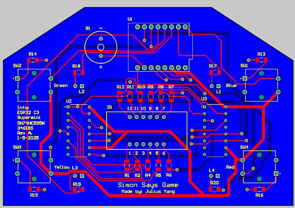
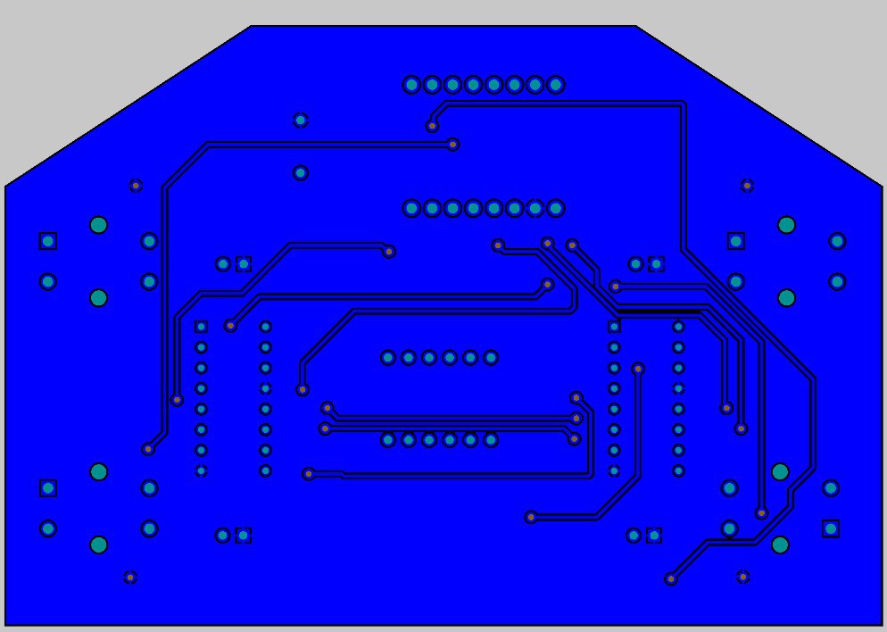
Since my board is a 2-layer PCB I did the standard top layer for signals, and bottom layer for the ground plane. If my signals had to cross one another, I used a via and routed the signal on the bottom layer, ensuring that a channel was created for it through the ground plane. For the most part I used the same trace widths except for the 3.3V line which was wider than all of the other traces. I probably could have gotten away with a narrower trace, but since this was the power line I wanted to ensure that there was enough current to power all of my components.
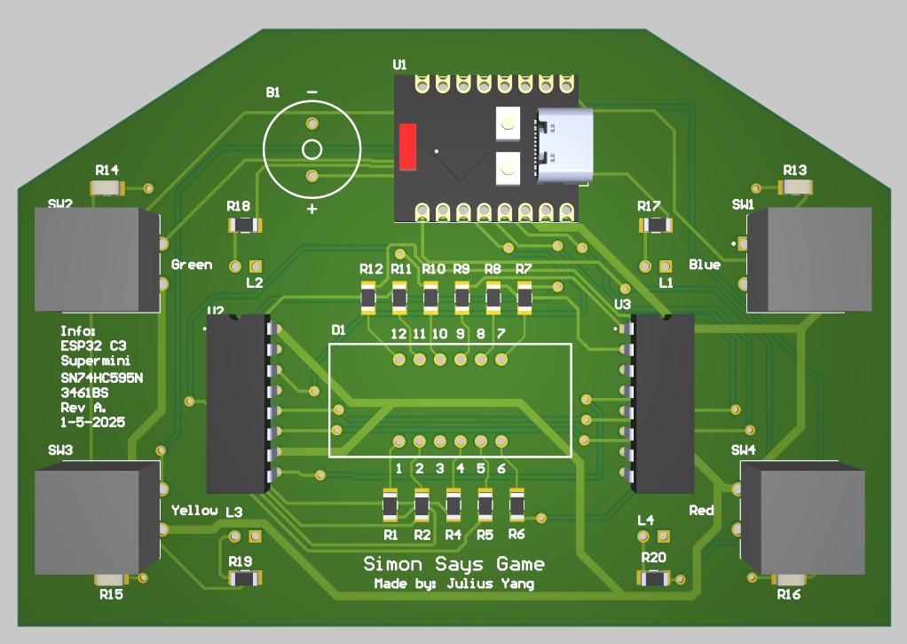
After all of the placement and routing this is what the final PCB looks like on Altium! All there is to do is to order my components and to fabricate the PCB
This was done between January 3, 2025 and January 5, 2025
Discussions
Become a Hackaday.io Member
Create an account to leave a comment. Already have an account? Log In.