Background

The concept of Hidden HID was born after I noticed how much space was available inside the USB connector and wondered if it would be possible to hide a rubber ducky completely inside it. With the increasing miniaturization of components, it was quite easy to design a basic USB enabled microcontroller circuit that fits inside the 2.5mm available. The device is kept in place using the phototransistors, which at 1.8mm tall are large enough to act as spacer elements. Added to the 0.4mm PCB, the resulting total thickness is 2.2mm, which fits snugly but comfortably inside the USB port. 

Once inserted, it can be removed again by inserting any thin plastic tool into the port and pulling on the phototransistors. I use a plastic tweezer that I broke in half :)
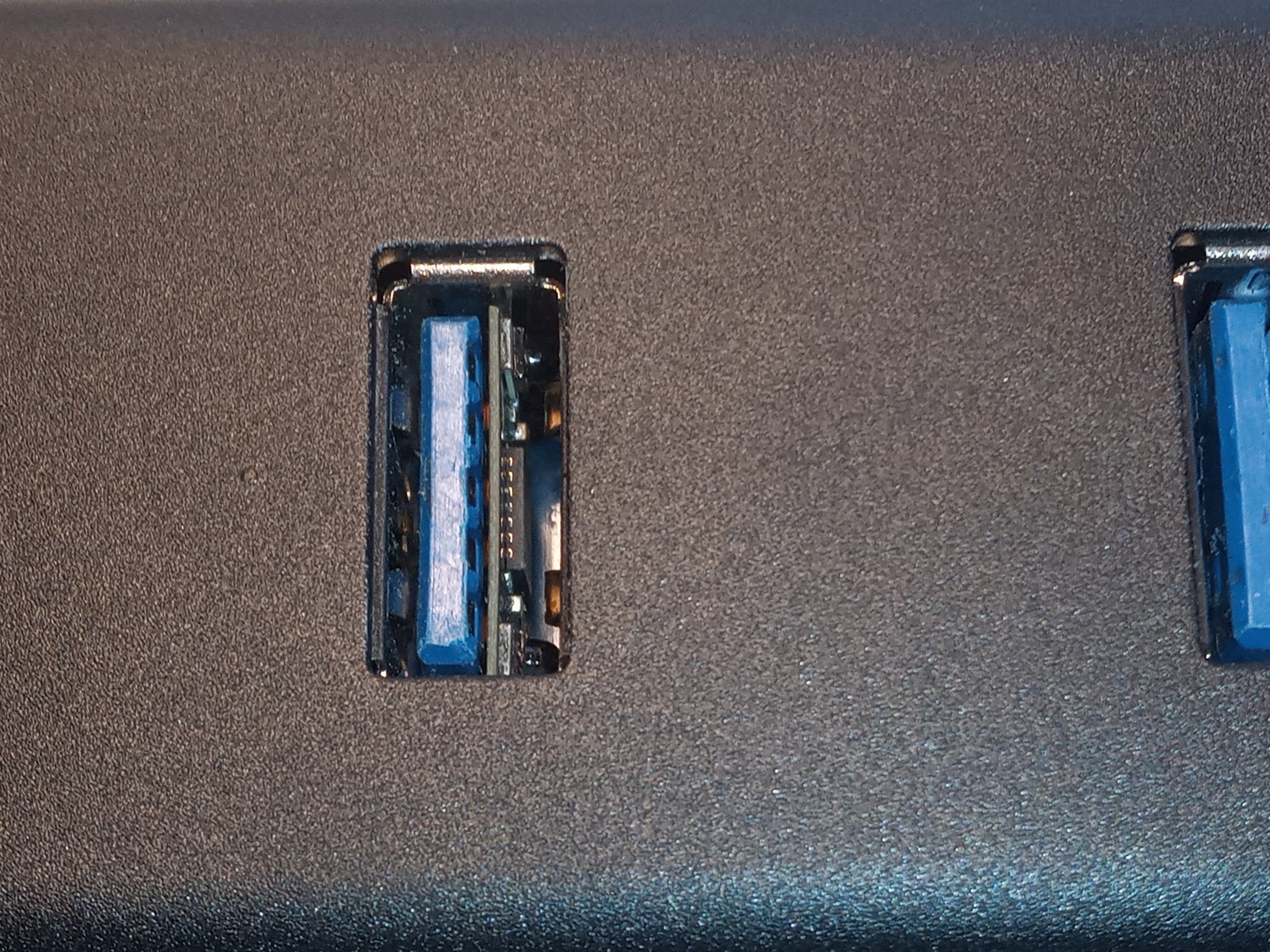
Close-Up of Hidden HID PCB inside a USB hub

View of the bottom side from inside a USB connector

Circuit

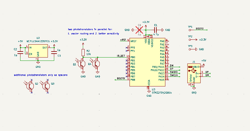
Screenshot of schematic
The circuit is very simple and similar to v1. The STM32F042 provides the USB functionality and even includes an internal 48MHz crystal, helping to minimize component count. The LDO steps down the 5V USB supply to 3.3V for the STM32. Two of the four phototransistors connect to the ADC of the STM32; the other two could not be connected due to routing limitations and are used only as spacing elements.
R2 was originally 2.2k but after testing I found that 10k provided a better sensitivity.

BOOT0, 3.3V and GND connect to test points to allow switching between bootloader and application.

PCB

I kept the PCB thickness at 0.4mm as this seemed to work well in v1, being robust enough to not bend while thin enough to remain inconspicuous. 

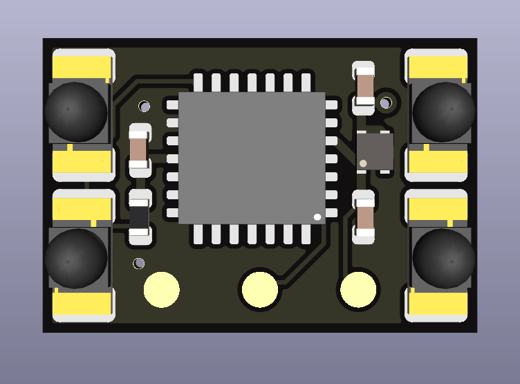
While developing v1 I was unsure how many  spacer elements would be required for stability, so had simply included a very long pad on each side of the PCB so that I could try out different configurations myself. This decision backfired, as my limited soldering skills meant the spacers were soldered unevenly, leading to an unreliable USB connection that sometimes worked and sometimes didn't. For v2 I therefore added IPC3 footprints for the phototransistors and included them in the BOM. 

3D model of v2 PCB
I ordered the boards from PCBWay, who have been my go-to PCB supplier for over a year now. I have been consistently impressed with the quality of the boards and of the customer service, which is both friendly and extremely quick. Order processing begins almost immediately and technical queries are sorted within hours.

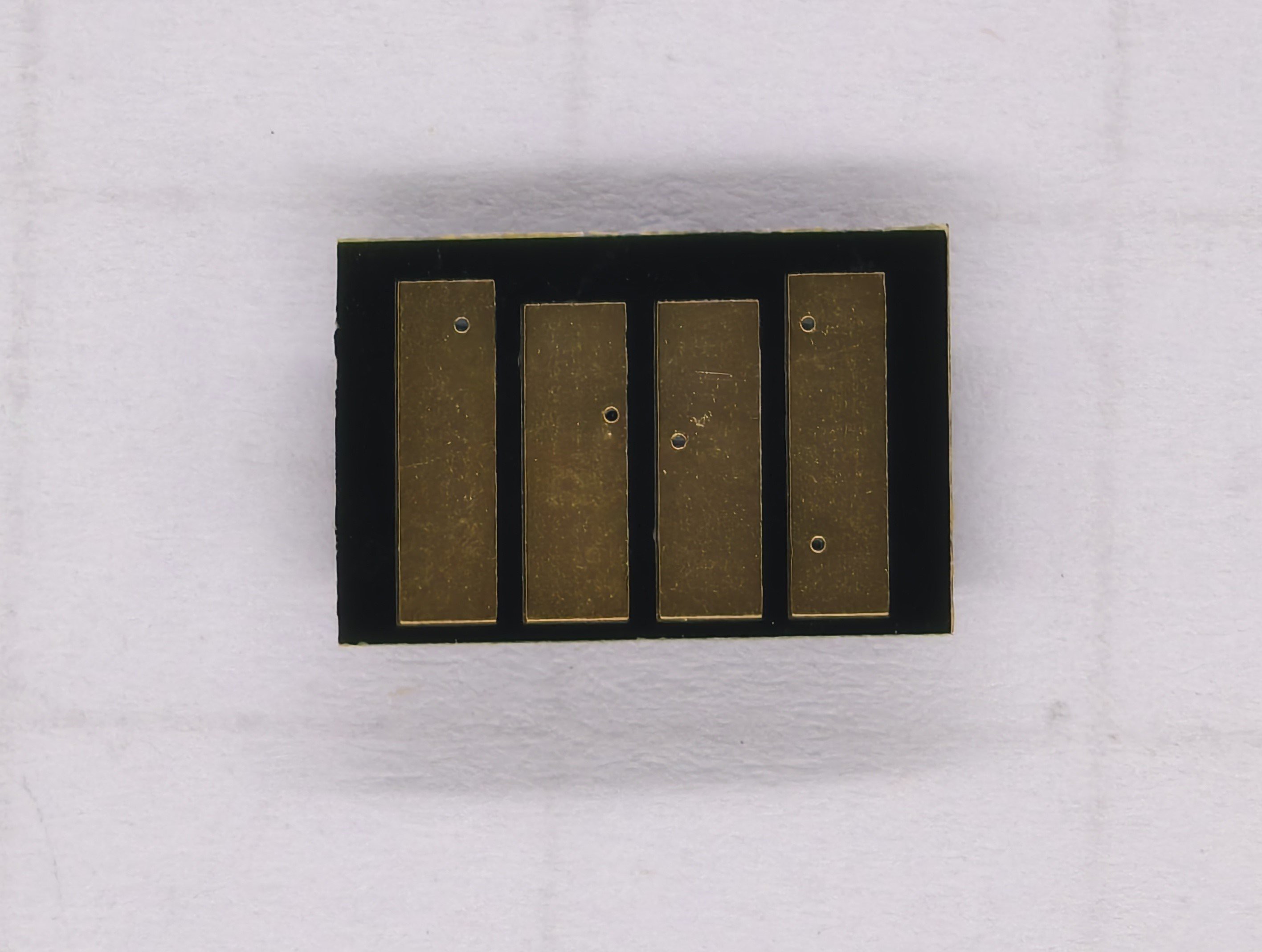
The small form factor and high component density made this PCB a little more technologically demanding than my previous orders from PCBWay but, as the photos demonstrate, this did not affect the quality of assembly or fabrication. 
bottom side of assembled PCB showing all components
top side of assembled PCB showing USB contacts
After ordering the PCBs, I discovered that I had made a mistake while researching the phototransistors. The particular model that I chose, 1541201NC3060 from Würth, is intended to be soldered upside down, with the lens poking through a hole in the board. I had never come across this form of assembly before and it was not clearly indicated in the datasheet, so I had assumed they were standard SMD components. PCBWay informed me quickly of the error and luckily were still able to hand-solder the transistors the way I needed them, so the design could still be completed. 

Frustratingly, I have not been able to find a good alternative phototransistor that fulfils the height requirements while allowing normal automated assembly.


Bring-up and Results

I had three goals for this revision: 1. to improve ease of programming and reprogramming. 2. to improve reliability of the USB connection and 3. to implement an on-off remote control using phototransistors. Let us address each point in turn:

1. Ease of Programming

To program the STM32, I use the 3 circular SMD pads at the front of the board. In the middle is the BOOT0 pin, on the left is GND and on the right is 3V3....
Read more »