 Aditya56h
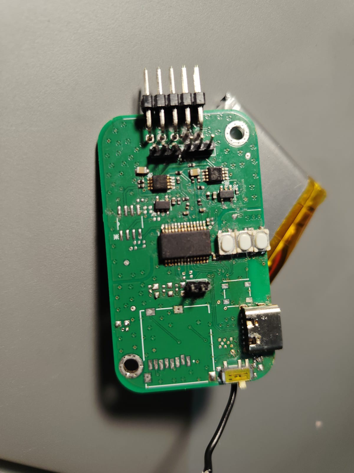
The first revision of the boards worked well (there was an issue with the analog frontend PCB). I have designed and populated a new PCB with STM32WB55MMG module and a battery charging module included with the MCP3912 frontend as a single PCB. I think this idea of a singular PCB is better than the stacking version of the project. Right now the PCB size is a bit big (I want to test all functionalities). The battery charger part works and I am able to program the STM32WB55 module using DFU mode via USB-C for now. I have some components left to arrive. I will then continue to develop the firmware for this board and then work on final version of this project. I have placed a limit of 35x35 mm board size limit for that revision. In my previous design I realized I didn't need all the channels from MCP3912, so now I am using half the channels. Interconnecting mezzanine connectors had tendency to rip the traces (I pulled the boards apart too hard).

Discussions
Become a Hackaday.io Member
Create an account to leave a comment. Already have an account? Log In.