Welcome to our build log, we would like you to join us on our journey in designing a USB voltage indicator. You will discover the complexity involved, the many hills and sometimes, mountains we had to climb to arrive at our USBVSense. IT was a long journey, but a wonderful voyage of discovery from the very start. Welcome and enjoy the ride
Features & Specifications
Fully capable of the latest USB PD EPR specifications (48 V, 5 A, 240 W)
A wide operational and measurement range of 4.5 V to 51 V
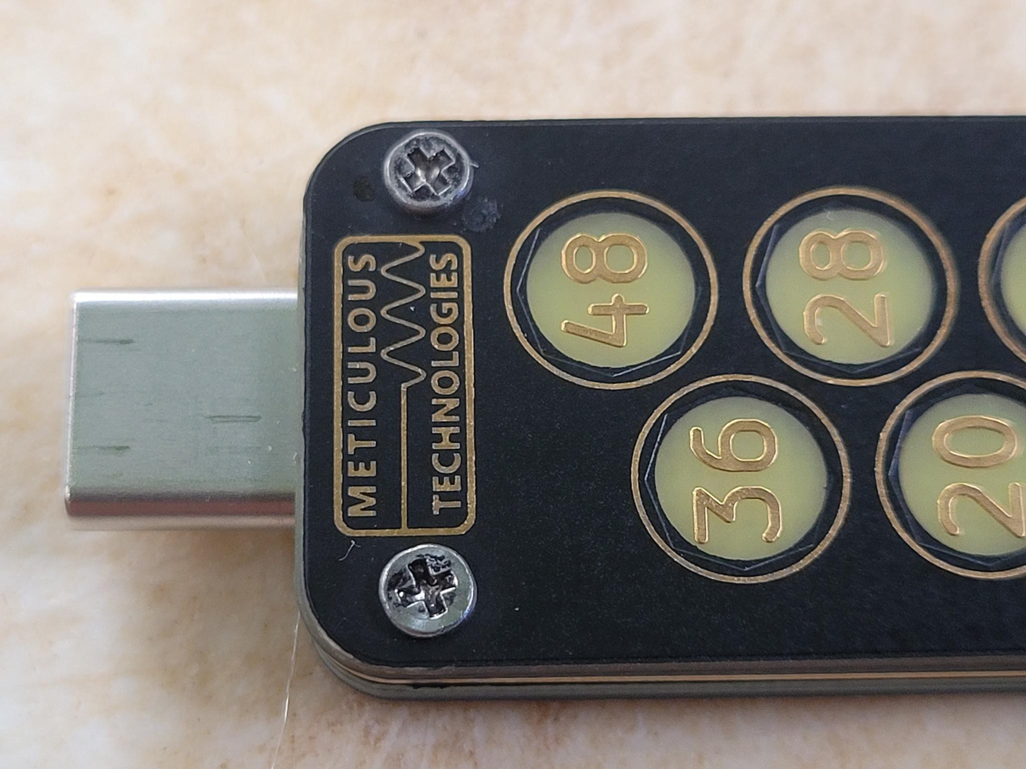
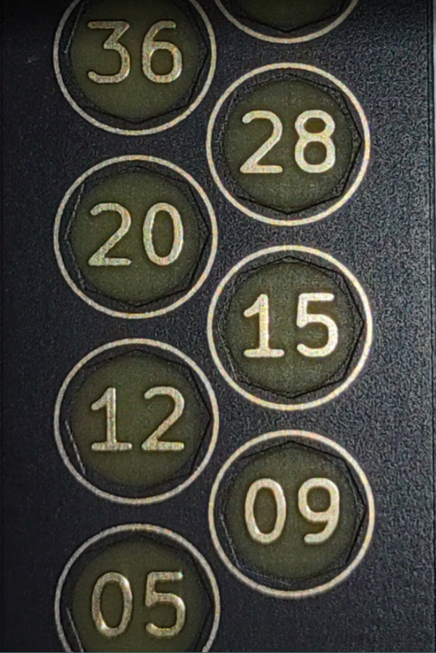
Individual color-coded indicators for each fixed voltage level:
5 V (red)
9 V (orange)
12 V (yellow)
15 V (green)
20 V (lime)
28 V (blue)
36 V (purple)
48 V (white)
Distinct alerts show > 5% and > 10% deviations from the fixed voltages. This feature is also helpful in approximating PPS voltages
Passthrough for USB 2.0 data, CC, and SBUS lines
Ultra-low power consumption, less than 6 mA of current drawn by the device (absolute maximum under regular operation)
ATtiny 406’s 10-bit ADC with 4.3 V internal voltage reference provides stable measurements of up to 22 mV resolution for voltages below 20 V and 49 mV for voltages between 20 V and 51 V
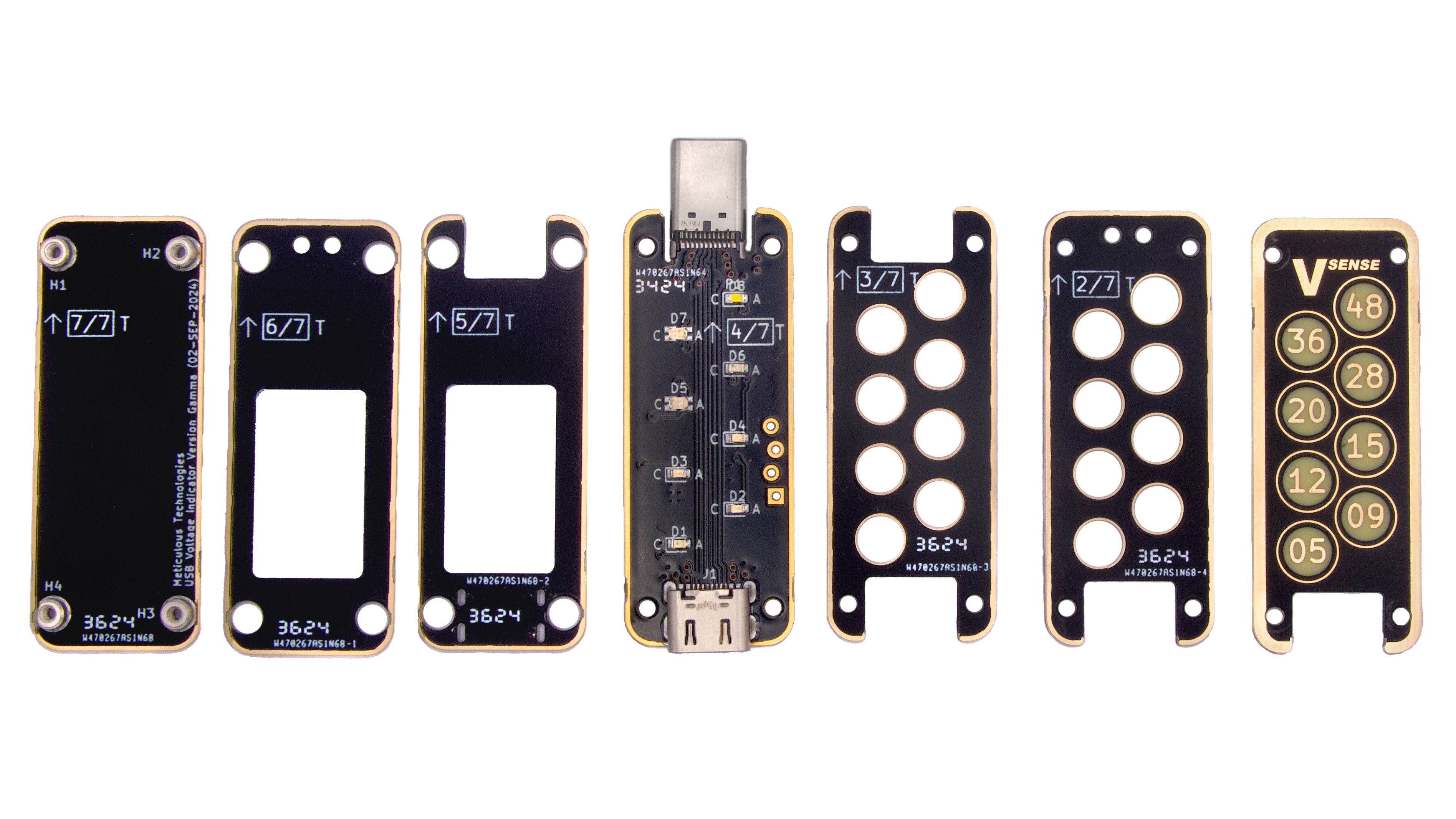
Stacked PCB construction with high-quality parts built to last:
Automotive grade LDO from Microchip (+70 V absolute max input voltage with ESD protection)
Kingbright low-current LEDs
JAE USB Type-C connectors rated for 48 V and 5 A
Dimensions: 56 x 18.5 x 5.6 mm (2.28 x 0.73 x 0.22 in)
The following table demonstrates the range of lights and flashing patterns and what they mean:
Voltage Range
State of Annunciators
Lower than 10% of 5 V (E.g. 4.4 V)
5 V (red) rapidly blinking
Lower than 5% of 5 V but higher than 10% (E.g., 4.7 V)
5 V (red) slowly blinking
Higher than 5% of 12 V but lower than 10% (E.g., 13 V)
12 V (yellow) steady and 15 V (green) slowly blinking
Higher than 10% of 12 V but lower than average of 12 V and 15 V (E.g., 13.4 V)
12 V (yellow) steady and 15 V (green) rapidly blinking
Within 5% of 15 V (E.g. 15.1 V)
15 V (green) steady
Lower than 10% of 20 V but higher than average of 15 V and 20 V (E.g. 18.5 V)
15 V (green) rapidly blinking and 20 V (lime) steady
Lower than 5% of 20 V but higher than 10% (E.g. 19.5 V)
15 V (green) slowly blinking and 20 V (lime) steady
Above measuring capability (E.g. 52 V)
48 V (white) rapidly blinking
Design Files:
We intend to make USB VSense fully open-source as soon as possible, we intend on publishing all the design files, including KiCAD project files, MPLABX project files, parts list, assembly instructions, etc. (Anything that is needed to manufacture and or customize USB VSense), as soon as we are done with our Crowd Supply campaign.
Current Status
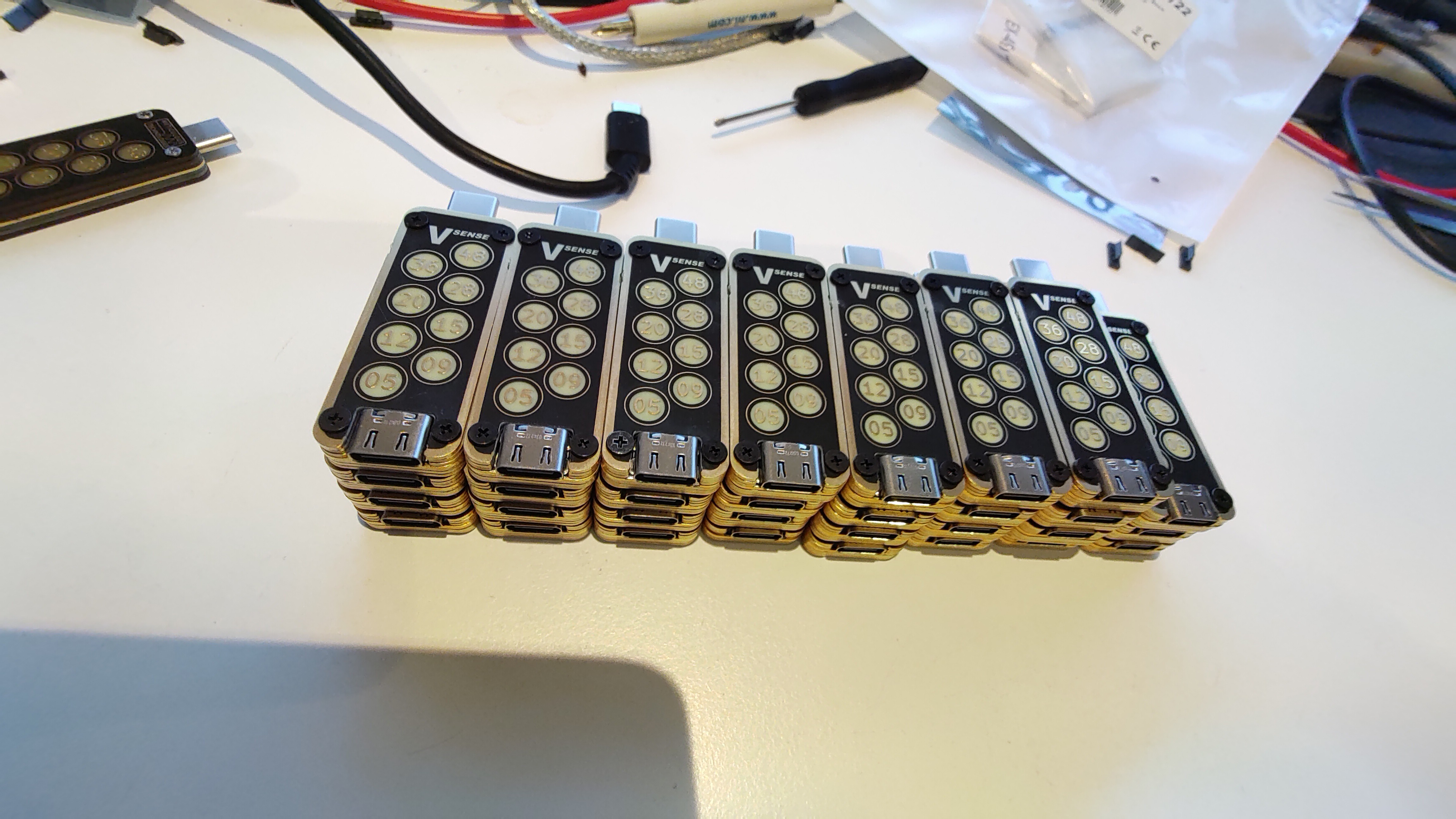
Small production run of 32 units has been completed with satisfactory results
Design Vision
The Design vision of USB VSense directly stems from the mission statement of Meticulous Technologies, which is, if we were to summarize it in one sentence, is to "Deliver top-quality electronics, which meaningfully adds value to the lives of those who use it, and freely share knowledge while in the process of doing so", thjat's why we intend all current and future projects to be fully open-source.
Currently, there is no shortage of USB meters in the market with endless lists of features, therefore, we conceived of a device that focused on only essential features for USB power diagnostics while still being useful to most users. We stuck to the keep-it-simple design principle as much as possible throughout the design process. What we would lose in terms of features we hoped to gain in terms of ergonomics, compactness, aesthetics, manufacturability, durability, and robustness, we also aimed for the device to be as easily as possible customizable by the user.
The very first decision we made was to not use a display to display the USB voltage, instead we opted for simple color-coded LED based indicators (annunciators), one for each of the standard USB-PD fixed voltages. This meant that the device could be a lot smaller in width while retaining the same readability of a device twice the width but with an LCD or an OLED display. Needless to say, this not only reduced the design complexity and reduced the overall costs but also streamlined the manufacturing process as well as significantly increasing the durability and robustness. Usually in a device an LCD display tends to be the part which is most fragile and is susceptible to damage from mechanical shocks and stresses, with no LCD there is no need to worry about getting one cracked or scratched. This also eliminates the need for additional manufacturing steps or instruction. However, by using a couple of LEDs it was impossible to display the voltage with any accuracy, to mitigate this we came up with a creative method of notifying the user of any voltage deviance from the fixed power delivery voltages, this was done by flashing LEDs, where the rate of flashing indicates the magnitude of the deviation.
Next, we decided to go for, what is called, a stacked PCB "Oreo" construction, in other words the enclosure of the device is formed by stacking several PCBs on top of one another, instead of a plastic enclosure, which is normally manufactured separately and requires a CAD design from a different software. Comparatively, all the PCBs can be manufactured together in one place and requiring only the PCB manufacturing files, which can often be generated from a single design file. With a PCB it's much easier to get a sleek metallic look which is hard to get with plastic without requiring additional processing, thus improving the aesthetics.
We are living in a world where the cost of a single PCB is as low as $5, this opens endless possibilities for the end-user to customize the looks of the device to suit their tastes, from changing the color of the device by changing the color of the solder mask, and they can change the style of numerals and even the shape of the indicators.
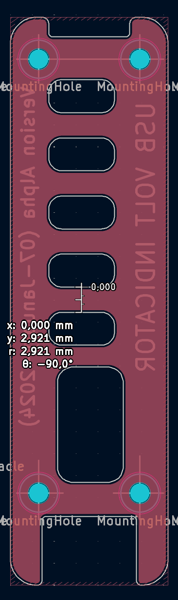
Alpha Design
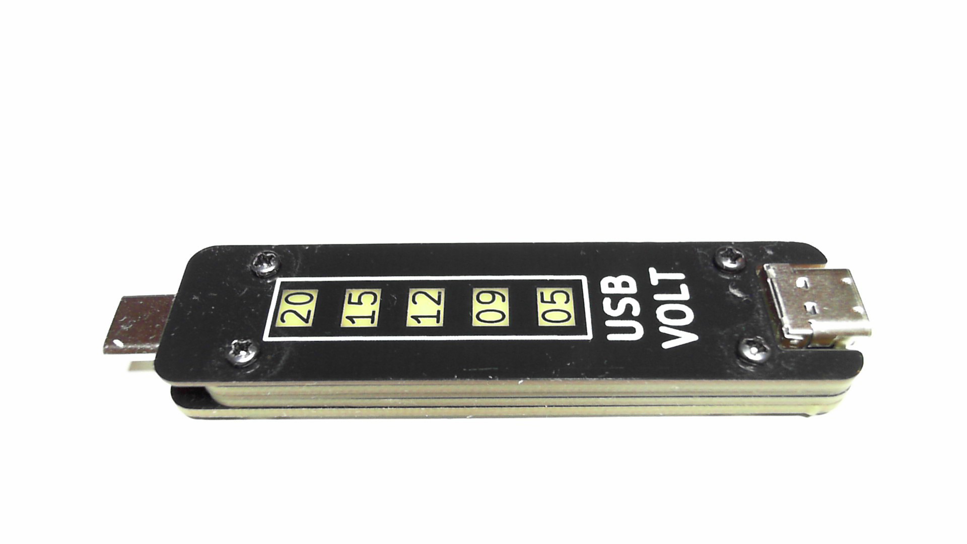
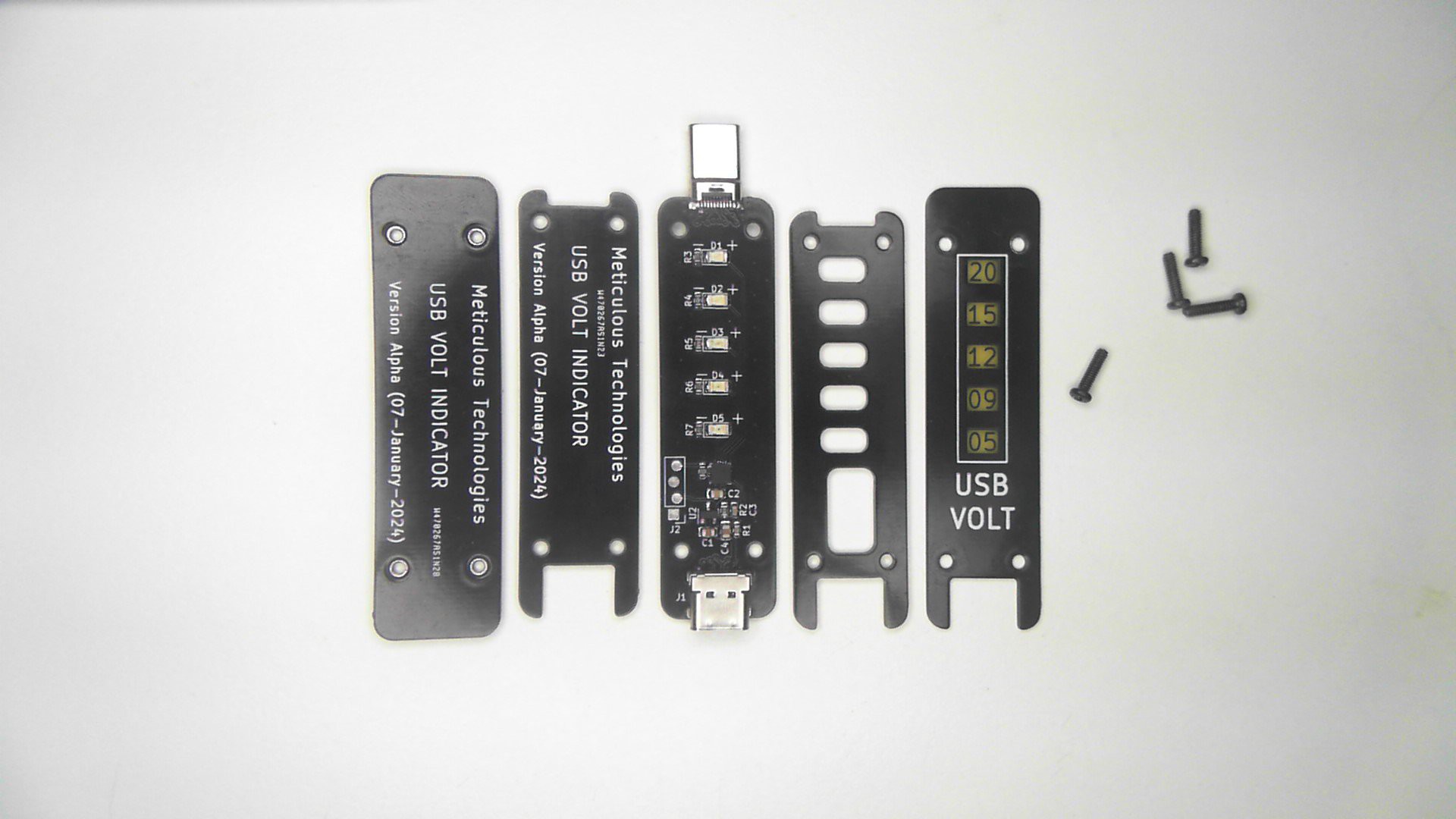
This was our first attempt at implementing our Design Vision, this version consisted of 5 PCBs, three PCBs with 1.6 mm thickness, and two with 0.8 mm thickness which were situated in the middle and at the top. The middle PCB was a 4-layer which was required for the impedance matching of USB data lines, the middle PCB also needed to be 0.8 mm to be compatible with the majority of USB-C plugs out there. The top PCB was chosen to be 0.8 mm as well, to allow the maximum amount of light to get through with minimal amount of color distortion. The overall length of this version was about 80 mm including the USB-C plug.
Design challenges and concerns (Alpha)
The first major challenge of this version was coming up with a reliable / sturdy method of holding together all the PCBs, to form one solid device with as little protrusion as possible.
It required the lowest possible power consumption which is required if we wanted to get away with using a simple LDO instead of a buck converter.
Finding components that would fit inside the cavity created by the cutting holes in a single PCB with margins to spare. That means no component could be more than 1.4 mm in height
Finding a good USB-C receptacle and plug that would be sturdy and is capable of 20 V and 5A. Specifically the USB-C plug needs to be as sturdy as possible since this component is expected to bear the most mechanical stress, since this is normally first to break in case of an accident.
A PCB design that would be able to handle a minimum of 5 A current.
To achieve a uniform brightness of LEDs of distinct color with as low a current consumption as possible.
We were concerned about the strength of the PCB after large chunks of it had been cut out to create cavities for the components. We had absolutely no clue how low we could go the width of PCB without significantly compromising its strength for the purpose or whether there will be any manufacturing issues due to it.
We weren't sure about how much clearance components needed, since they must fit within the cutout in a PCB, this is sometimes dependent upon the precision of component placement (reflowing does not always reposition the components) and the milling accuracy of the PCB manufacturer.
We wanted to include an indication for 5% voltage deviation; therefore, we were concerned about resolution of the measurement since we were measuring up to 22 V. Therefore, the ideal voltage resolution would be about 25 mV, which is an order higher than 0.25 V (5% of 5V).
Solutions (Alpha)
After a lot of research we decided to go with screws on one end and threaded steel spacers (SMST series by Wurth Elektronik) on the other end to hold the entire device together, although we weren't sure about the strength and reliability of the solder joints, because it could depend on the quality of the PCB and SMT process.
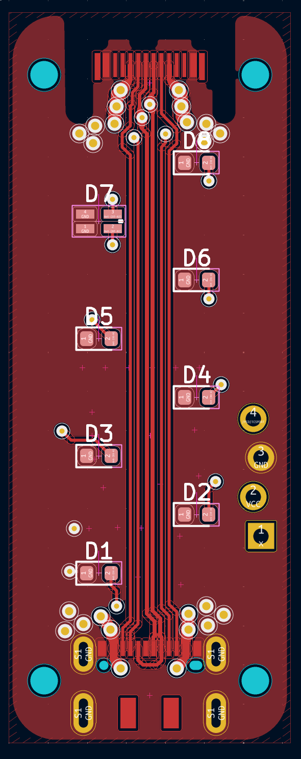
Every good PCB design starts with choosing the optimal PCB stack-up, after some thought we decided to go for signal, ground, power, signal (bottom to top). This way the high-speed signals on the bottom layer can be adjacent to ground plane to achieve the required impedance matching as well as the power planes (VBUS and GND) can have two fully dedicated layers which would help ensure 5 A current specification with minimizing PCB width.
We thought Kingbright's low current LEDs would be ideal for the ultra-low, power-consumption requirement of our device. These LEDs offered light intensity of 24 mcd and more at a current of just 2 mA. Calculations showed that even with all LEDs on at the same time power dissipation in the LDO would be no more than 176 milliwatts at 21 V input voltage.
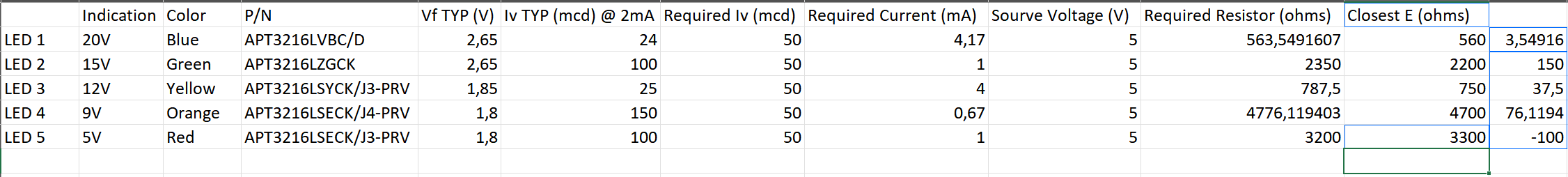
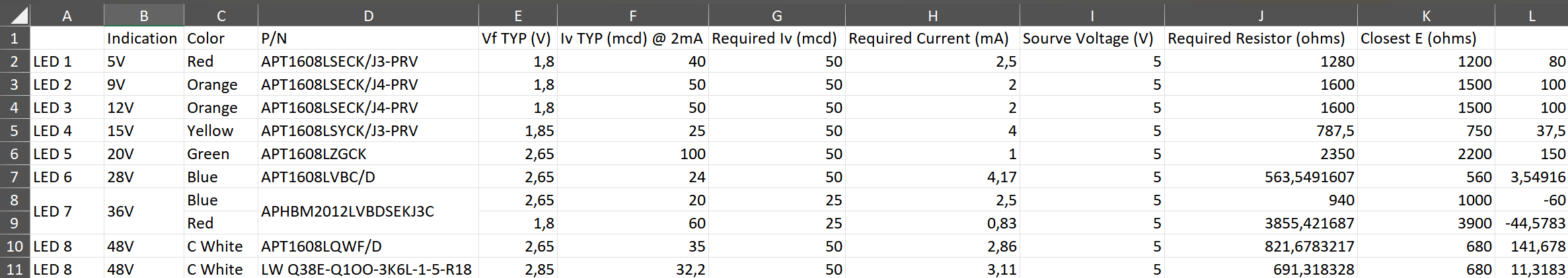
The table below presents the calculated current-limiting resistor values required to achieve uniform brightness across all indicators, targeting a light intensity of 50 mcd for each LED. It is to be noted that datasheets of red and orange LEDs had two ambiguous values of typical Intensity in them, we weren't sure which one to use so we went with the higher one, this would have consequence later.
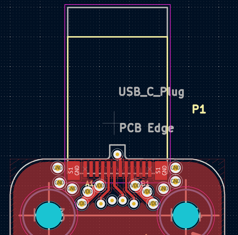
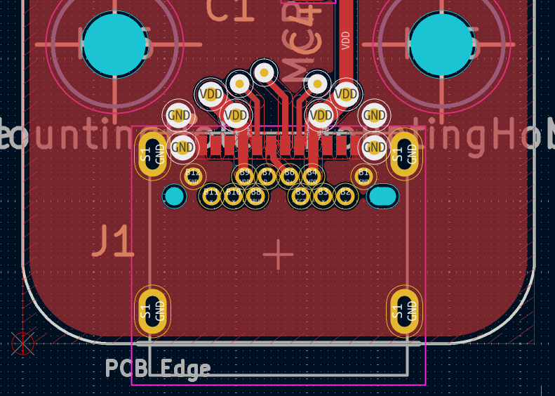
Since we wanted to be sure that the PCB can handle 5 A of current at a minimum, we took results out of Saturn PCB Toolkit and doubled the numbers for extra margin or tripled them wherever possible. This was done for both minimum track width and via sizes. As already mentioned, two entire layers were dedicated for power. Furthermore, special attention was paid to via placement. The following images show the placement of vias around the USB connectors.
For this design version we were extra careful about the minimum width of the PCB (after cutouts) which was kept at a minimum of 2.5 mm and the cutouts were made large enough so that PCB edges would be well outside of the component courtyards.
Design Evaluation (Alpha)
When the first of the Alpha prototypes arrived, it was no surprise that the design had no faults, and they were fully functional given how simple the design was.
Questions Answered
One of the first things we noticed was how well all PCBs fit together with plenty of margin between the components and cutout edges. Furthermore, the PCB with the cutouts was sturdy, even after applying quite some force by hand it didn't come anywhere close to breaking. This alleviated all of our concerns regarding the mechanical aspect of our design and we realized that the cutouts didn't need to be any larger than the area under component courtyards (according to the footprint standards), and that we have a lot of room to play with; the minimum width of the PCB edges, which was quite generous.
Another pleasant realization we had while evaluating this design was how well-lit all the indicators were. There was minimal color distortion (only slight color distortion for blue and green and no noticeable color distortion of other colors) and all the colors were as easily distinguishable as looking at LEDs directly. All the indicators were mostly evenly lit with excellent light distribution resulting in total visual comfort, as would be in the case of a purpose-built light indicator.
Problems Discovered
The very first problem we noticed with the Alpha design was that the red and orange LEDs were significantly dimmer than the rest. Fortunately, it was easy for us to figure out why that was so. Previously we mentioned that the datasheets of red and orange LEDs had two ambiguous values for typical intensity, and we went with the higher values, we were quite sure that in the next design if we choose the lower one, this problem would be solved.
The second problem we noticed was light bleeding from one indicator to adjacent indicators, as it's clear from the following video clip:We thought if we could avoid light bleeding or at least minimize it, which could result in a much nicer and cleaner look, as well as improve the legibility of the indicators.
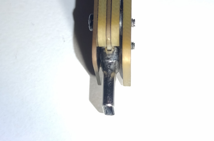
The third problem was that there was too much space above and below the USB-C plug, as seen in the following pics:
This was a severe problem for the durability of the plug. With nothing to securely limit the plug from bending when the device is plugged in, all the rotational forces on the device would have to be endured by the solder joints of the plug. It would only be a matter of time before it failed.
The dimensions of the device might have looked good on paper. However, at 80 mm in overall length the device was way too long, and formed an excellent lever waiting to get broken by accident. Needless to say, this was far from our design vision of a small compact device. This was unacceptable!
Finally, we felt that the voltage measurement of up to 20 V was just not sufficient anymore, we saw plenty of devices such as power banks taking advantage of recently added extended power range (EPR) to USB power delivery. The EPR added three additional voltages to already existing four fixed voltages to USB power delivery. We thought that it was prudent to add these to the USB VSense.
Beta Design
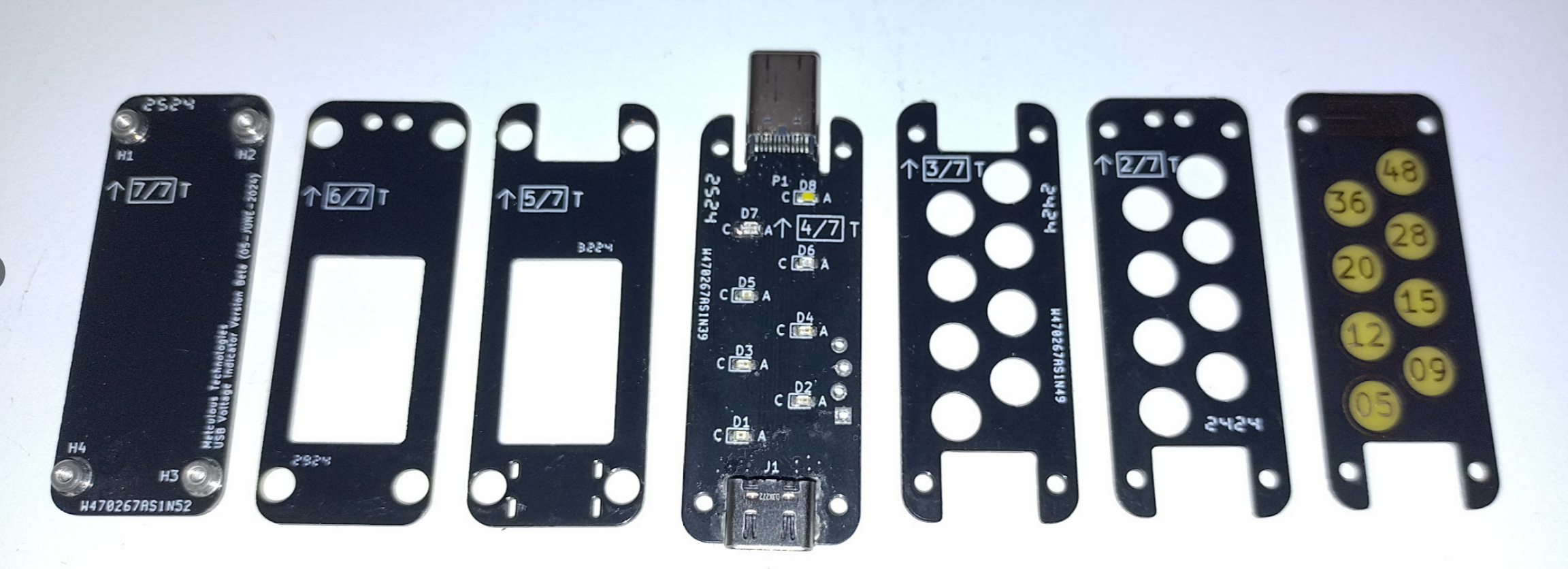
The Beta Design was a major improvement over our Alpha Design; both in terms of size, added voltage indicators and aesthetics. The number of PCBs used in this version was increased to 7, compared to 5 in the last version. However, all the PCBs were of the same thickness i.e., 0.8 mm, resulting in the same overall thickness of the device as the previous version. the consequences of this improvement made for easier producibility.
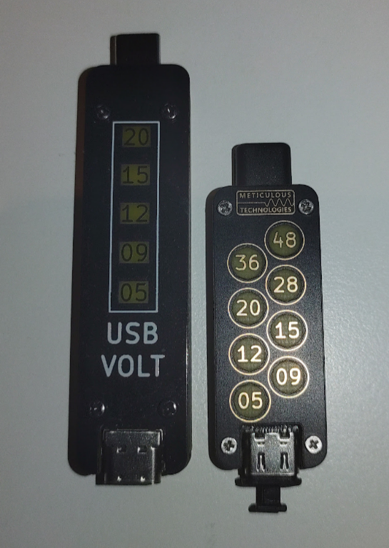
The overall length of the device was reduced from 80 mm down to 56 mm, while three additional voltage indicators were added to cover the EPR voltages, as seen from the following picture showing Alpha and Beta design side by side:
Side by side comparison of Alpha and Beta versions
Design challenges and concerns (Beta)
A Significant (at least 20%) reduction in the overall length of the device while adding three additional indicators.
Three additional indicators would require three additional unique colors, which may not be possible with a single-color LED.
Modifying the design to tolerate input voltage of up to 60 V at the very least while still being functional at 4.5 V, since normal operating conditions of the device would now include voltages of up to 52.8 V (48 V + 10% of 48V).
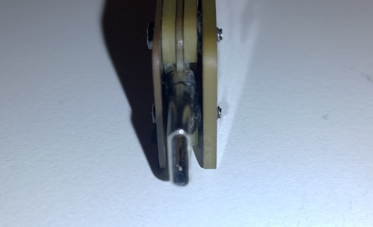
Reducing the gap around the USB-C to minimize how much it's allowed to flex, which would in turn minimize the mechanical stresses on the solder joints of the plug.
With the voltage measurement range now being (4.5 V to 52.8 V) even with the 10-bits ADC of the ATtiny, voltage resolution would be 48 mV, when ideally it should be 25 mV.
Aesthetic improvement
Solutions (Beta)
The first and most intuitive modification to the previous design was to place components on both sides of the "main" PCB, as opposed to restricting them to one side, this could result in added cost of manufacturing but after consulting with PCBWay we thought it was well worth it, given the reduction in length. So now, all the LEDs can be placed on the top while the rest of the components (other than USB connectors) can be at the bottom, this would also considerably improve the aesthetics of the device by eliminating any empty spaces leading to a more symmetrical look. Placing components on both sides would also have an unintended consequence that the high-speed or other passthrough signals won't have a dedicated layer, we will address this issue in the next step.
Next, we decided to change the shape of the indicators from rectangular to circular and arrange them in a zigzag pattern. Circular indicators would mean that they could be placed closer to each other at a 45-degree angle, this would also decrease light bleed. Both changes would not only result in a great reduction in length but as well much better look for the device. As mentioned in the previous point that passthrough signals would no longer have a dedicated PCB layer, but thanks to placing indicators in a zigzag this wouldn't be necessary! Both passthrough signal LEDs can be on the same layer while the signals retain their straight and shortest path from receptacle to plug (as shown in the figure below). The stack-up of the "main" PCB was changed to Signal, Ground, Power, Signal (from top to bottom).Zigzag placement of indicators allows the high-speed signal to pass straight though the middle
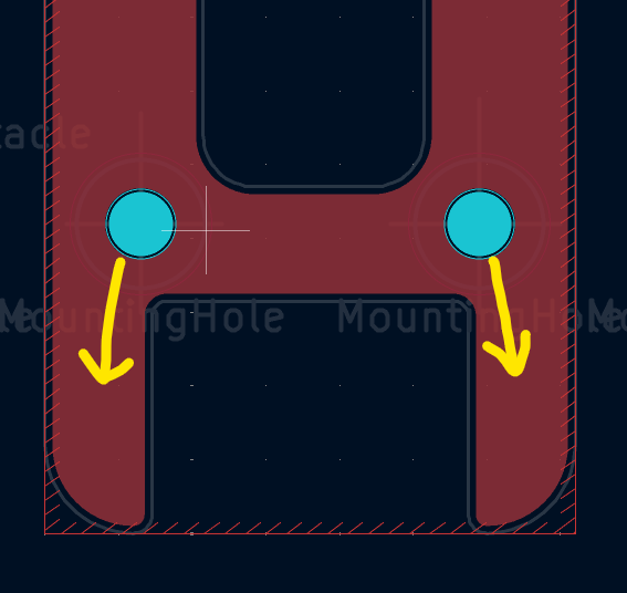
Another major change was that we reduced the size of the screws from M2 to M1.6, primarily so that the screws, screw holes and threaded SMT spacer can be placed adjacent and "in-line" with the USB connectors, again reducing the overall length of the device.
In the Alpha design the screw spaces contributed to the additional length
In the Beta design we got rid of the extra length by changing the position of screws
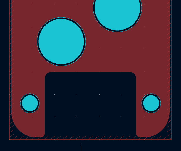
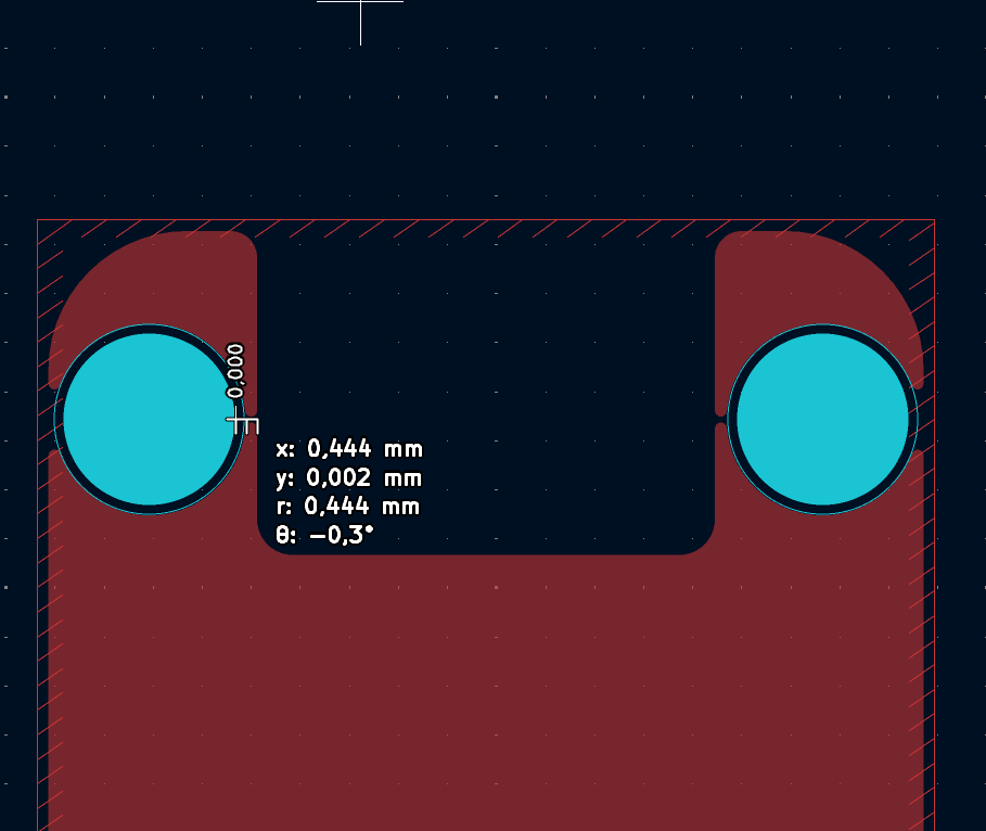
This however had an unintended side effect that it required one of the PCBs to have a width of less than 0.5 mm in some places, which is less than 500 micrometers!!! as shown in the figure below. This is because two PCBs were required to have holes much larger in diameter than what would be required for a M1.6 screw, so that entire SMT spacer could fit inside them, leaving absolutely no protrusion on the outside or gap between the PCBs (another improvement in the beta design).We had no clue if this would work or the PCB would just fall apart either during the manufacturing process or while handling, in the previous design we tried to constrain the PCB width to 2.5 mm on a 1.6 mm thick PCB, however now we were trying to push it to less than 0.5 mm on a PCB that was half (0.8 mm) as thick. However, after consulting with PCBWay we decided to go further with this idea. I guess we'll only know for sure when we have the manufactured PCBs in our hands.
Finding the parts designed to work with 48 V was harder than expected. The first problem was finding an LDO capable of accepting an input voltage range from 4.5 V up to 60 V, with a package height of no more than 1.4 mm. We were fortunate enough to find one from Microchip (MCP1792T-5002H/CB), which had an absolute maximum voltage of 70 V, had ESD protection and was able to endure unwanted voltage transients, which we thought was quite neat for our purpose. Finding USB-C connectors that were rated for both 48 V and 5 A was no easy task, we wanted to avoid the ones that would require special assembly instructions or require a PCB that couldn't be manufactured using Quickturn facility. Finally, we settled for the USB connectors without pins for USB super-speed signals manufactured by JAE.
In the previous version it was possible to find low-current single LEDs with unique colors, with Beta design requiring three more indicators it won't be possible, so we had to get a little bit creative here. First, we thought of using a white LED, however Kingbright did not have a white low current LED (not one that was available anyways). So, we looked for alternatives and we found an OSRAM alternative, although we weren't sure if white would be distinguishable enough from yellow after it has been color distorted by the FR4 material. Further, we decided to use same color (orange) for both 9 V and 12 V indicators, our rationale was that since 12V is no longer a standard fixed power delivery voltage, there would rarely be a scenario where both 9V and 12V are used simultaneously. Finally, Kingbright did have low current bi-color LEDs with two possibilities, either red and blue (forming purple) or blue and green (forming lime). We thought lime might be difficult to distinguish from green, so we chose the former. The following image shows the implementation:
In Beta version 9 V and 12 V indicators are both orange colors, while white and a bi-color (purple) LED was added for 48 and 36 V indicators
Finally, the current-limiting resistor values were recalculated for the Beta version to ensure consistent illumination levels across all LED indicators.:
Updated current-limiting resistor values (Beta)
Another problem we had to address was the fact that increasing the voltage measurement range from 22 V to 51 V would result in degraded measurement resolution from 22 mV to about 50 mV (when the ideal is about 25 mV). To avoid this, we decided to split the voltage range into low (from 0 to 22 V) and high (from 22 V to 51 V) range and use different ADC pins connected to separate voltage dividers for the two ranges. This would work because the minimum voltage deviation higher voltage will be used to detect is 1.4V (5% of 28V), as opposed to 0.25V for the lower range.A major downside of this approach was that voltage on the low range ADC pin would exceed VCC voltage when the input voltage (VDD in the above figure) is higher than 25 V, to mitigate this, we tied both the pins to VCC using a Schottky diode which would limit the voltage on the ADC pins to rise to a maximum of 5.4 V (approx.), we further calculated input current in those pins in case of an open-circuit diode failure and made sure that it was well within the maximum acceptable values of the input current given in the ATtiny's datasheet. Of course, implementing the two-range solution would require the software to be slightly more complicated, but it is well worth it.
Lastly, we had to solve the problem of that USB-C plug "flapping around in the breeze", the goal was to reduce the gap at the top and bottom of the plug as much as possible. There were two solutions that we could think of, the first that we solder something (like a SMT gasket) on the adjacent PCBs to fill up the gap, however the downside of this approach was that it would not only increase the parts count but also would require component assembly on two additional PCBs. The second possible solution was to change the 5 PCB design to a 7 PCB design; this will reduce the gap at on the top and on the bottom by 1.6 mm in total (0.8 mm on each side), the major advantage of this method was to make all PCBs of the same thickness (0.8 mm), this would allow the 6 two layer PCBs (out of 7 in total, the middle one has to be 4 layer PCB) to be manufactured as one panel, reducing the cost and ordering complexities. (Note, in the Alpha version the bottom most PCB was also 1.6 mm, however since in Beta version we changed to M1.6 screws, the SMT threaded spacers could fit within a 0.8 mm PCB). The results are shown in the images below:
the Alpha version: The USB-C plug was much more exposed with quite some gap on the top and bottom
The Beta version (left), the Gamma Version (right): Gap on the top and bottom of the USB-C was reduced to almost zero
Several aesthetic improvements were made in this version, including much more rounded corners, and significant improvements to the numerals. In the previous version numerals were black, since they were part of solder mark, in this version they were etched in copper allowing for an ENIG finish, resulting in a sleek gold look.
Design Evaluation (Beta)
As soon as we got our hands on the manufactured beta version, it was again no surprise that the device was perfectly functional as intended. We loved how nice the device felt with its much-reduced size and refreshed look. We decided to test this version as extensively as we could, since we were confident that this version was quite close to something that we were willing to release to the outside world. Among other things, we meticulously tested the device for accuracy, its ability to carry current (ampacity) and thermal margins.
Questions Answered
First thing we were curious about was how accurate the device was. We used ATtiny's internal 10-bit ADC for taking the measurements. As it turns out, the three Beta version devices we tested had an error of less than 50 mV at around 5 V, this included the 22 mV Schmitt threshold voltage programmed in the software for avoiding the device being in an astable state. This error seems to increase proportionally with input voltage to about 100 mV at 20 V, it was obvious what we were looking at was the ADC gain error. The good thing was that as the gain error increases so does the 5% and 10% voltage tolerances. So, we concluded that the accuracy of the device was sufficient.
Next, we wanted to know if the device was actually capable of carrying 5 A current. To test this, the plug side of the device was connected to a USB-C breakout board with shorted VBUS to GND, the receptacle side of the device was connected to a power supply via a 5 A rated USB-C cable and another USB-C breakout board.The power supply was in a constant current mode set to 5 A. After turning on the power supply it took about 5 to 6 minutes for the device to reach thermal equilibrium, however the device was barely warm. This looked quite promising to us, so we increased the current to 6 A (the power supply's maximum), and after another 10 minutes our device got slightly warmer. We thoroughly looked for any localized hot spots, however there were none, the device was uniformly warm. Satisfied by these results we proceeded to measure voltage drop across the entire setup, which came to be about 200 mV, combined with 5 A current this mean total (loop) resistance was approximately 40 milliohms (including the resistance of cable and 6 connectors etc.) which was excellent, since the maximum allowed loop (VBUS + GND) resistance of a 5A cable as per specification is 150 milliohms (Section 4.4.1 IR Drop, Universal Serial Bus Type-C Cable and Connector
Specification, Release 2.4, October 2024). The only problem now was we did not know how much resistance our device contributed to the total resistance of 40 milliohms; to figure that out we took out our device from the test setup and plugged the adapter with VBUS shorted to ground direct to the USB-C cable and measured the voltage drop again. This time around the voltage drop came out to be about 100 mV, half of the previous value. This meant that our device contributed to a resistance of about 20 milliohms. This is again great since it meant that most USB-C cables would remain within the USB specification with our design plugged in unless they were manufactured at the very edge of the specification of 150 milliohms.
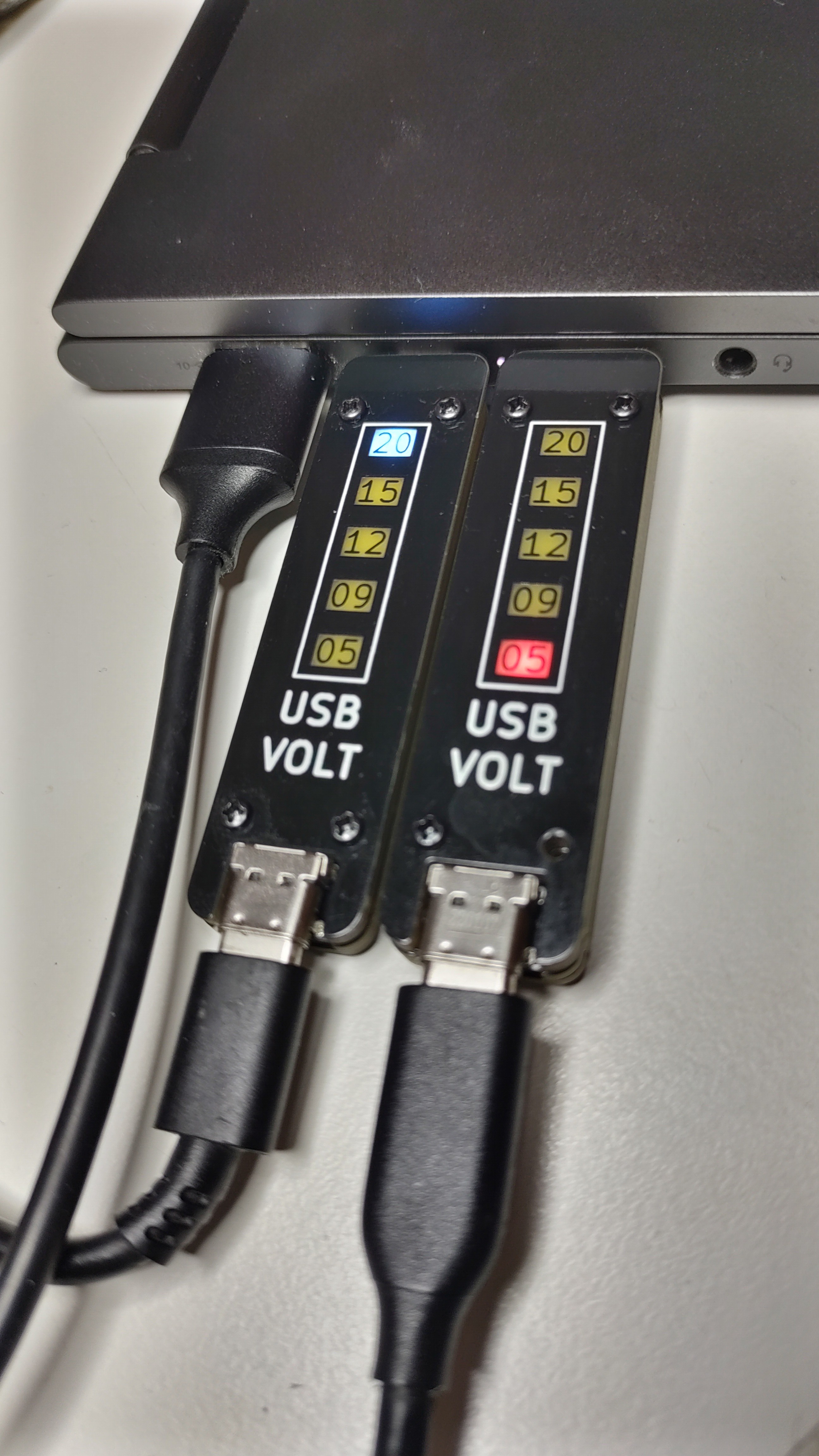
Now that we were satisfied with the ampacity of our device, the next question was; could the LDO endure the abuse of having an input voltage of 51 V while providing enough current for the device to function as intended. To answer this question, we decided to set some baseline first. So, we decided to test with input voltage of 51 V with all the LEDs on!!! This would draw a total of about 25 mA current resulting in power dissipation of 1.15 W, there was no way that a LDO with a tiny SOT-23A package could handle that much power dissipation for more than a couple of minutes at best, but the question was how long would it take for the LDO to hit the max junction temperature, of course our LDO had the automatic thermal shutdown protection and recovery. So, we began the test, and it took just 2 to 3 seconds before we saw LEDs flickering, this meant that LDO had hit the max junction temperature within a couple of seconds. After some thought we decided that at the bare minimum the LDO should be able to tolerate an input voltage of 51 V together with a current of the three most current-hungry LEDs without hitting the max junction temperature, in normal operation only two LEDs could be on at the same time (one steady and one flashing), therefore, testing with 3 LEDs ON should give us enough margin. Consequently, we repeated the test with three LEDs on, and it was a success, LDO was able to achieve thermal equilibrium this time without hitting the junction temperature, we measured the current draw, and it was about 11 mA which means power dissipation of about half a watt. However, we thought that the LDO was too hot for our comfort. Since we were testing at an ambient temperature of about 31 C and it's reasonable to expect the device to be used at an ambient temperature of up to 50 C, this meant that we couldn't be certain if the device would work under all normal scenarios.
 Meticulous Technologies

 We had no clue if this would work or the PCB would just fall apart either during the manufacturing process or while handling, in the previous design we tried to constrain the PCB width to 2.5 mm on a 1.6 mm thick PCB, however now we were trying to push it to less than 0.5 mm on a PCB that was half (0.8 mm) as thick. However, after consulting with PCBWay we decided to go further with this idea. I guess we'll only know for sure when we have the manufactured PCBs in our hands.
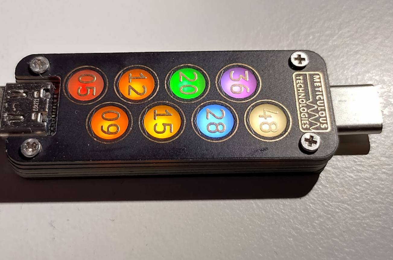
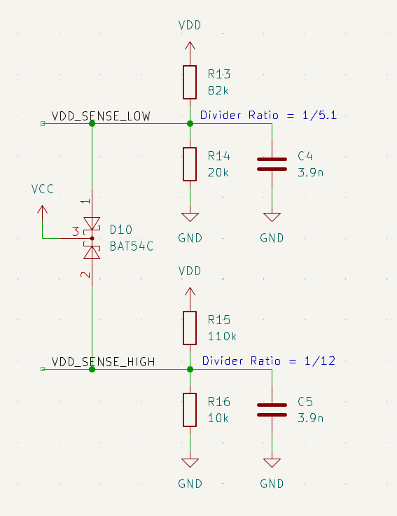 A major downside of this approach was that voltage on the low range ADC pin would exceed VCC voltage when the input voltage (VDD in the above figure) is higher than 25 V, to mitigate this, we tied both the pins to VCC using a Schottky diode which would limit the voltage on the ADC pins to rise to a maximum of 5.4 V (approx.), we further calculated input current in those pins in case of an open-circuit diode failure and made sure that it was well within the maximum acceptable values of the input current given in the ATtiny's datasheet. Of course, implementing the two-range solution would require the software to be slightly more complicated, but it is well worth it.
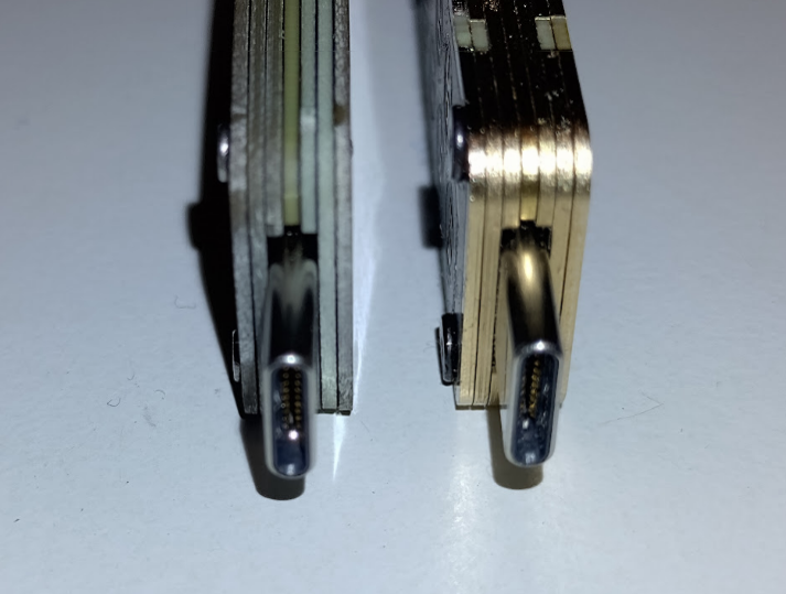
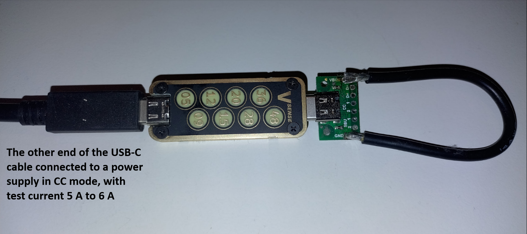 The power supply was in a constant current mode set to 5 A. After turning on the power supply it took about 5 to 6 minutes for the device to reach thermal equilibrium, however the device was barely warm. This looked quite promising to us, so we increased the current to 6 A (the power supply's maximum), and after another 10 minutes our device got slightly warmer. We thoroughly looked for any localized hot spots, however there were none, the device was uniformly warm. Satisfied by these results we proceeded to measure voltage drop across the entire setup, which came to be about 200 mV, combined with 5 A current this mean total (loop) resistance was approximately 40 milliohms (including the resistance of cable and 6 connectors etc.) which was excellent, since the maximum allowed loop (VBUS + GND) resistance of a 5A cable as per specification is 150 milliohms (Section 4.4.1 IR Drop, Universal Serial Bus Type-C Cable and Connector
Specification, Release 2.4, October 2024). The only problem now was we did not know how much resistance our device contributed to the total resistance of 40 milliohms; to figure that out we took out our device from the test setup and plugged the adapter with VBUS shorted to ground direct to the USB-C cable and measured the voltage drop again. This time around the voltage drop came out to be about 100 mV, half of the previous value. This meant that our device contributed to a resistance of about 20 milliohms. This is again great since it meant that most USB-C cables would remain within the USB specification with our design plugged in unless they were manufactured at the very edge of the specification of 150 milliohms.
The power supply was in a constant current mode set to 5 A. After turning on the power supply it took about 5 to 6 minutes for the device to reach thermal equilibrium, however the device was barely warm. This looked quite promising to us, so we increased the current to 6 A (the power supply's maximum), and after another 10 minutes our device got slightly warmer. We thoroughly looked for any localized hot spots, however there were none, the device was uniformly warm. Satisfied by these results we proceeded to measure voltage drop across the entire setup, which came to be about 200 mV, combined with 5 A current this mean total (loop) resistance was approximately 40 milliohms (including the resistance of cable and 6 connectors etc.) which was excellent, since the maximum allowed loop (VBUS + GND) resistance of a 5A cable as per specification is 150 milliohms (Section 4.4.1 IR Drop, Universal Serial Bus Type-C Cable and Connector
Specification, Release 2.4, October 2024). The only problem now was we did not know how much resistance our device contributed to the total resistance of 40 milliohms; to figure that out we took out our device from the test setup and plugged the adapter with VBUS shorted to ground direct to the USB-C cable and measured the voltage drop again. This time around the voltage drop came out to be about 100 mV, half of the previous value. This meant that our device contributed to a resistance of about 20 milliohms. This is again great since it meant that most USB-C cables would remain within the USB specification with our design plugged in unless they were manufactured at the very edge of the specification of 150 milliohms.