The artwork
As my username implies, I really love drinking (club) mate. I therefore decided to make my PCB art mate-themed: the PCB outline should resemble a mate bottle, with the labels featuring some custom art. As the medium of the art is a PCB, there should be additional considerations when creating the artwork. A PCB consists of multiple layers. Each layer has it's own color and special properties.
Silkscreen: The uppermost layer. Usually used to print component references. All boardhouses support white silkscreen, with some supporting printing black, when the soldermask is white. Silkscreen is only printed on top of soldermask.
Soldermask: The soldermask covers the copper and protects it from corrosion. The soldermask is usually green, however some boardhouses offer multiple colors.
Copper: The copper is etched to form traces in a PCB. The copper layer is the most interesting layer, due to the interaction with the soldermask. If you don't print soldermask on copper, the copper is exposed. The color of the copper depends on the manufacturing process. When using the standard HASL process, exposed copper will be covered in solder, looking silver. If you use the ENIG process, a small layer of gold will be plated, leading to a gold finish. The ENIG finish is also very smooth and planar, while the HASL finish features very small, but noticeable solder blobs. If there is soldermask on top of the copper, the soldermask color usually looks more "saturated". As the copper layer has some thickness, there is some room to play with haptics.
Substrate: The substrate is the core of the PCB and gives structural support. It is made from layered epoxy resin and fiberglass sheets (PCB lasagna?). When completely exposed (no copper, soldermask, silkscreen), it is yellow and quite opaque. Only one boardhouse manufactures PCBs with black substrate (OSHPark), to my knowledge. It is possible to backlight a PCB, when using side or reverse-mounted LEDs.
My idea was to make a back-lit bottle of mate. As mate looks yellow, exposed substrate would give some of the yellow color, while also letting through light from yellow LED mounted on the back. I decided to use exposed copper to outline the PCB and labels. To better the match the color, and for more bling-bling, I used the golden ENIG finish. On the big bottom label, I wanted to draw the mysterious guy featured on the club-mate label, with some pixel-sunglasses.
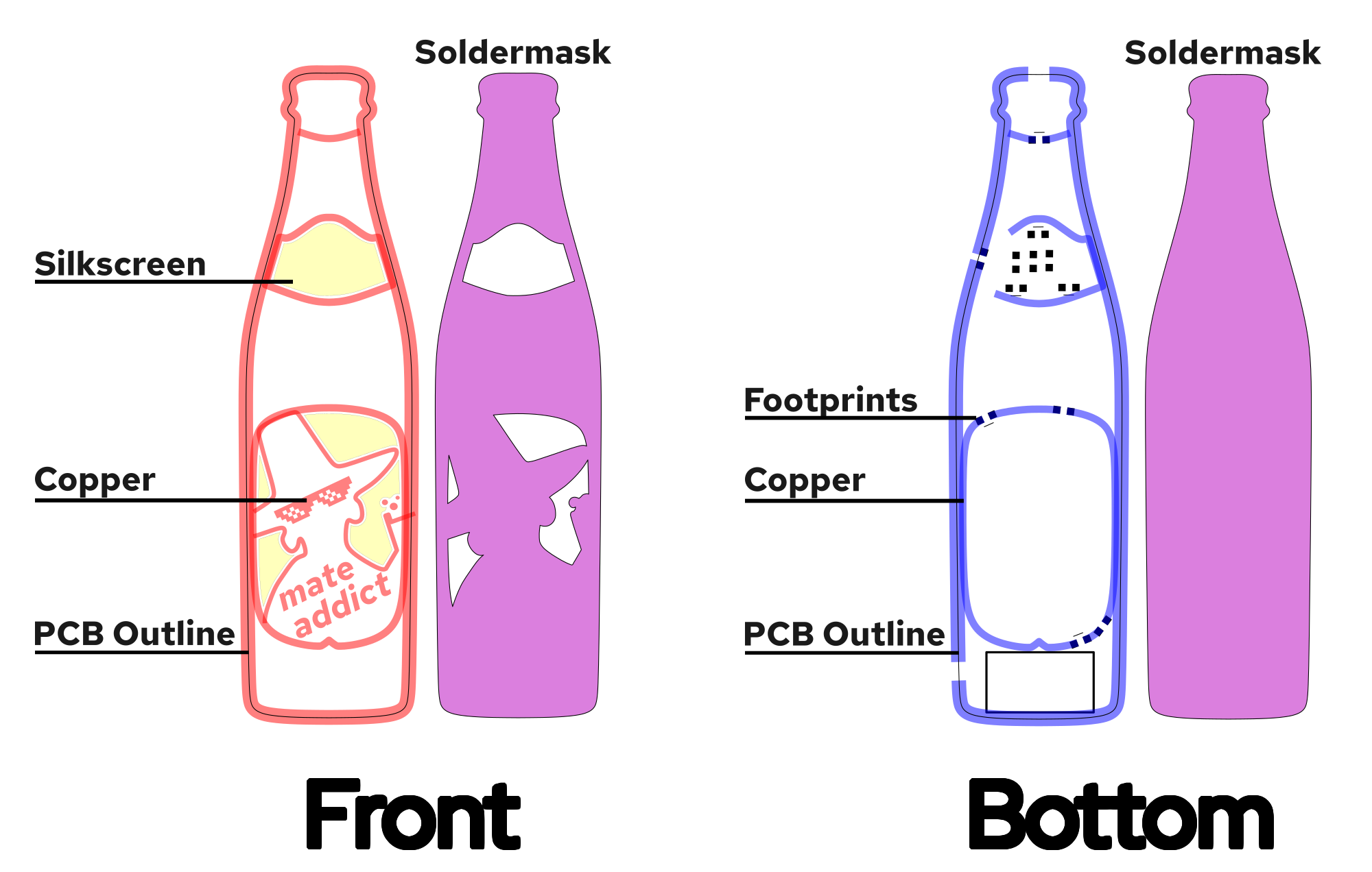
To simplify exporting to KiCAD, the PCB layers were separated onto Inkscape layers. The soldermask layer is "negative" and transparent spots would become green. To create a functioning circuit, I modeled the resistors and LEDs in Inkscape. I then copied the outlines from the top layers and cut it accordingly to create "pads" for the components. The footprints show in the picture were not exported. They were just used as reference.
Importing SVGs into KiCAD
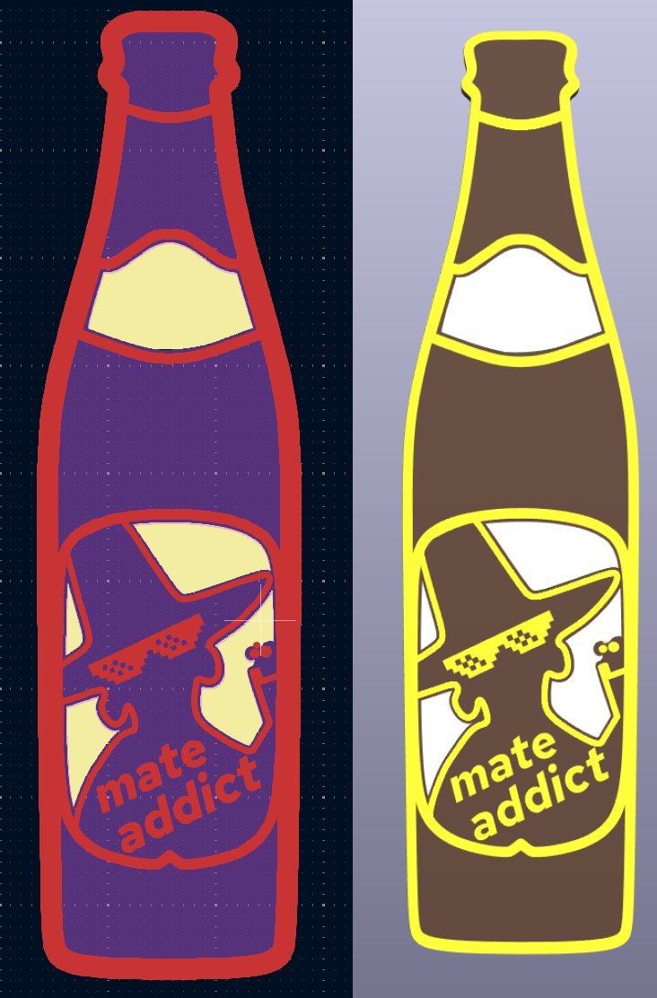
KiCAD actually allows a direct import of SVG graphics in the PCB editor (File > Import > Graphics) . The whole graphic is then put into one single layer. It looks like lines are converted to segments, while objects are converted to polygons. I recommend also grouping elements.
This is also the reason why the layers should already be separate in Inkscape. It is then quiet easy to export each single layer as separate .svg, and imported into KiCAD. Finally, the layer groups must be aligned. Unfortunately, the groups do not allow positioning in the properties tab. As a work-around, I selected a very fine grid and aligned the layers. This whole process is quiet manual, but fast. There is an option to import to a given location. However, the svg sizes must be identical then, so that they then end up aligned.
By the end, I was surprised how easy the process was. I tried multiple tools and extensions for KiCAD and Inkscape with poor results.
Routing the PCB
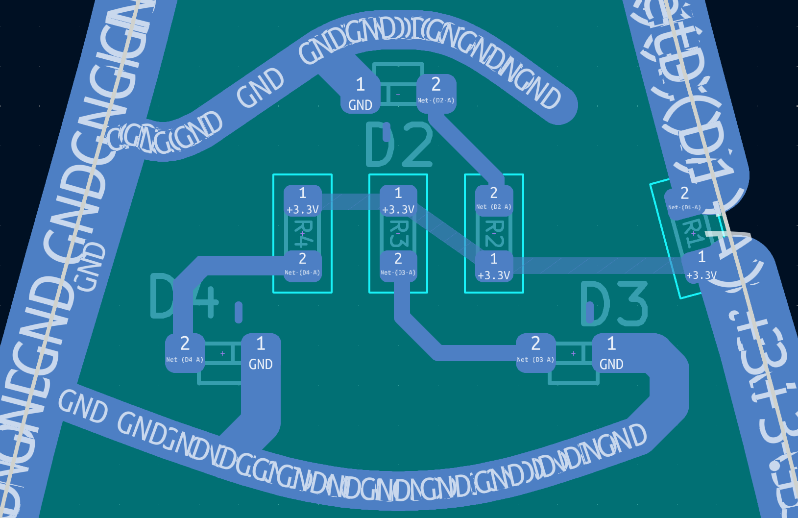
Last but not least, the LEDs, resistors and badge connector are routed. The segments and polygons of the copper layers are not assigned to a net after import. To do that, you just drag a components pad into the segment - then, all connected segments are assigned to the pad's net automatically. That's it! Even DRC works, and one can check for shorts / unconnected components.
When there are many short segments, the net labels get a little messy.
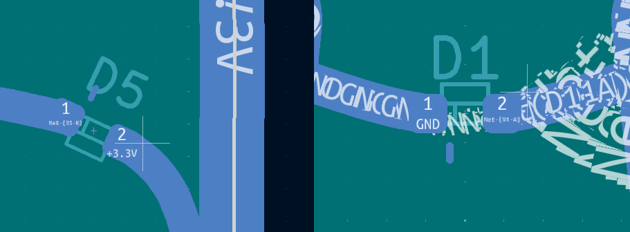
Some of the segments imported weirdly, and were too long. I guess that was a result of KiCAD resolving vector lines into multiple small segments. Excessive segments can be simply selected and deleted, to restore the original shape. All polygons KiCAD created, were accurate.
There are no restrictions when placing components or routing them. It is possible to route to and from imported segments and polygons.
PCB manufacturing and assembly
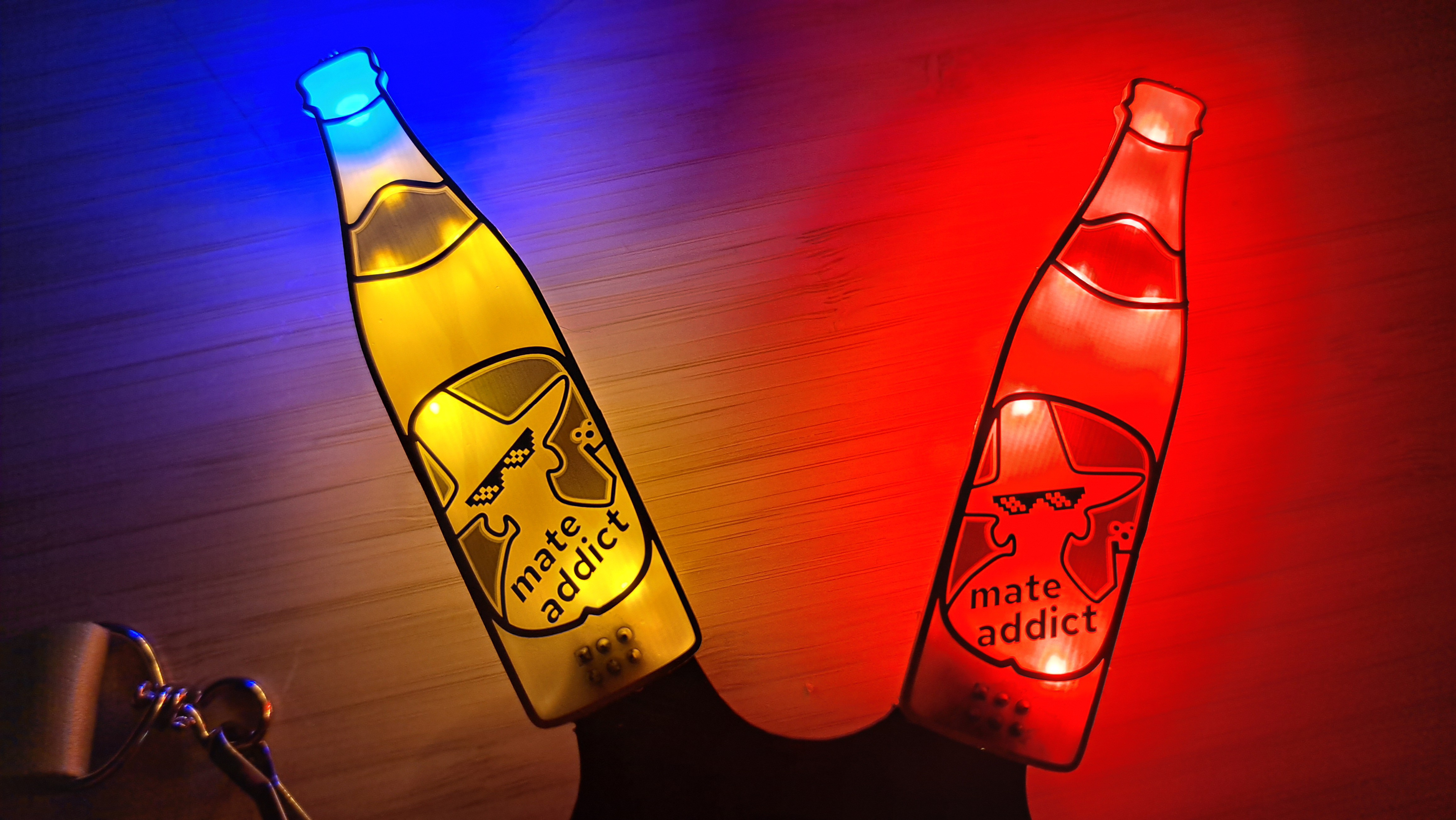
I choose the german PCB manufacturer AISLER, as their PCB's are of really good quality. They also offer a very nice PCB preview and KiCAD upload. To get the PCB before the event, I chose the express service and the PCB's arrived on time. The PCB's actually turned out really beautiful. As mate comes with different flavors, I ordered red, yellow and orange LEDs. For the characteristic blue cap, I used a single blue LED.
I assembled the PCB's in three different ways: hand soldering, hot-plate and reflow oven. The hand soldered PCB's kept their yellow substrate color. When assembling with a hot-plate or oven, the substrate becomes darker. One of the oven soldered PCB's now looks like a beer bottle!
To diffuse the light, hot glue is usually used. I initially didn't have hot glue, and I made the first diffusor with two component glue. The two component glue created a nice uniform coat.
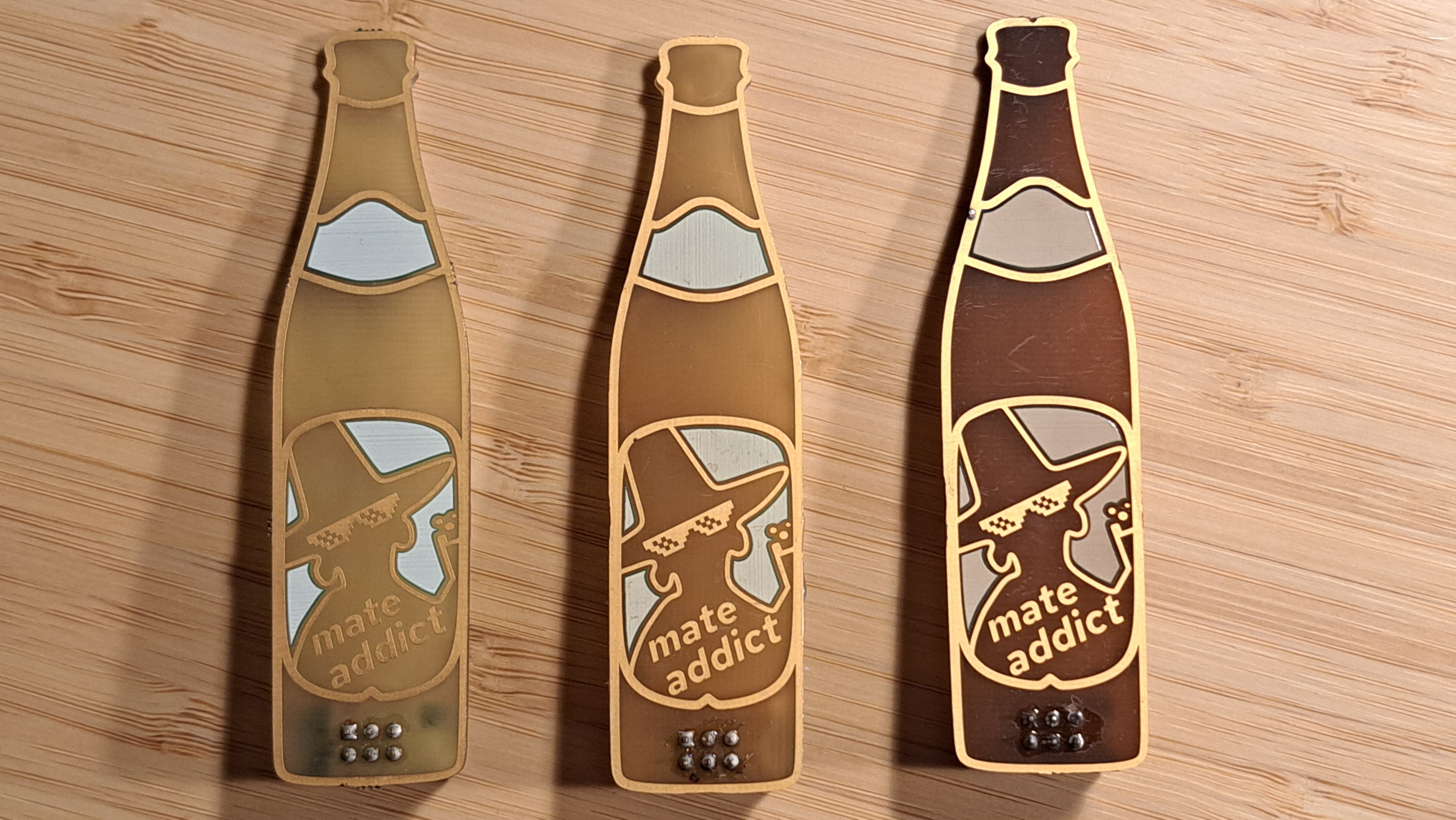
However, it is clear and did not diffuse well. Hot glue works better as a diffusor, as it is more opaque. It is however messy and does not look as clean. The ideal solution might be some kind of opaque epoxy resin, which would create a nice opaque coat.
 Daniel