 High Code
To be honest, we took a while to share updates here, but I promise I’ll catch you up quickly now.

Let’s start with the first PCB ever made for the High Boy. We spent quite some time studying the layout thinking about component placement, functional blocks, and the overall area for each section. I sketched a few drafts with what I thought were “compact” dimensions. Eventually, we finalized the schematic and sent it off to get our first prototype made.


Well… it came back — and we ran into quite a few issues. Not to mention the size — it ended up looking more like a Samsung S20 😅. But that’s okay, it’s all part of the journey.

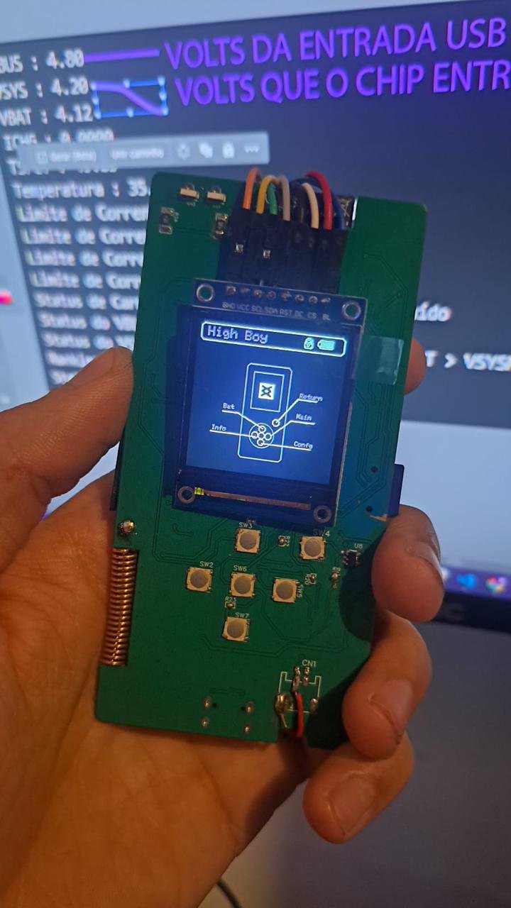
The important thing is that we learned a lot. We carefully marked every issue and took detailed notes so we can improve everything in the next revision.
Discussions
Become a Hackaday.io Member
Create an account to leave a comment. Already have an account? Log In.