 Tim
Tim
A classical DRAM only has few control lines
A0-A7        Multiplexed Address Lines
Din, Dout    Datain/out. These lines can be shorted together for bidirectional I/O
nWE          Write enable. When low, the selected memory cell is written to.
nRAS         Row Access Strobe - "Open" a row in the memory array
nCAS         Column Access Strobe - selecto which bits in the row to access.
A 64k*1 DRAM consists of a memory array of 256 columns and 256 rows. Each memory cell is made up of a transistor and a capacitor.
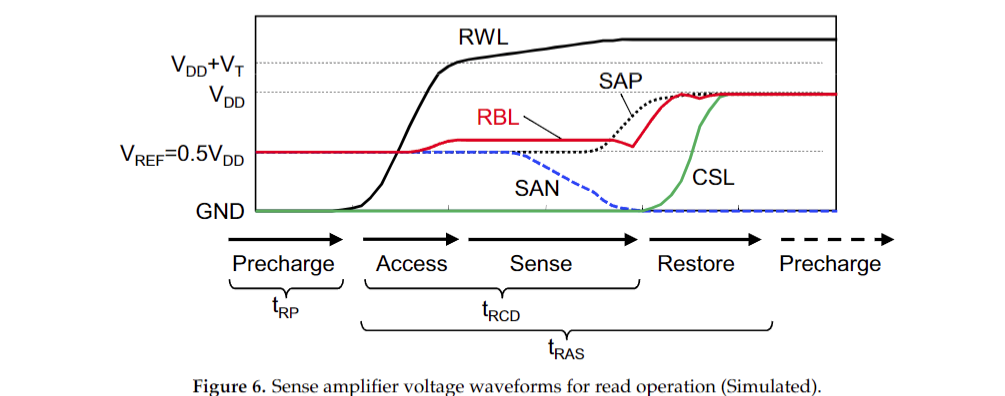
The core functionality of a DRAM is actually controlled by the RAS line. When it is pulled low ("Access"), the row indicated by the address pins is loaded from the memory arrray into the bitlines by activating the transistors in the memory cells. Since the charge on the capacitors is fairly small, the bitlines will only change their voltage slightly. However, at the same time the read amplifiers are activited, which will amplify the small voltage on the bitlines ("Sense") and pull the bitlines to up/down ("Restore").
This serves two functions:
1) It will amplify the bitlines voltages enough so that they can be sensed as a logical level.
2) At the same time, it is refreshing the charge on the memory cells.
In a next step, it is possible to complete the row access by pulling up RAS. That would complete a refresh cycle. After the RAS line is pulled up again, the "Precharge" cycle begins, where the bit lines are pulled to a reference voltage of ~0.5Vdd.
Alternativey, the RAS line can stays low and the CAS lines is pulled low in addition. This will allow reading from or writeing to one of the 256bits of the ROW.
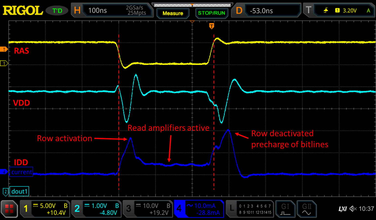
I used a transimpedance amplifier to measure the current consumption of a DRAM during the row access, as shown below. We can see a spike associated with the row activation, which likely stems from charging the wordline, which is connected to the gates of all transistors of the row we want to access. While RAS is low, we can see an increase current consumption from the read amplifiers. Once the row is deactivated, we can see another current spike that is associated with pulling low the word line and precharging the bit lines.
Now this is interesting - even if we only want to access a single bit in the DRAM, we actually have to load an entire ROW of 256bits from the memory array. So, why not do something with all 256bits in parallel?
Discussions
Become a Hackaday.io Member
Create an account to leave a comment. Already have an account? Log In.