 bru3s
bru3sAs mentioned in the project description, one of the driving forces behind the form factor of the PCB was that I had some products from M5Stack lying around unused, among which the original Core Grey and an expansion module called Faces (specifically the 2nd version), which adds some LEDs and a keyboard.

I specifically wanted to make a T-Deck-like device, so I set forth constraining the PCB dimensions and positioning of components to that.
A note on standalone mode
The project specifications included a "standalone" mode and a "module" mode; these are two ways the device can be used, depending on whether it's mounted as an M5Stack compliant device or not.
- In module mode, the RP2350 is treated as an SPI slave, receiving commands from the ESP32 core such as "set the power" and "transmit". In this mode
- The USB port is not used for power supply
- VBUS from M-Bus is used instead
- The RP2350 either interprets commands or acts as a passthrough to the SX1261
- it has no agency of its own (e.g. spontaneous transmission)
- LEDs are treated as simple device indicators
- user button events are relayed to the ESP32
- serial debug is still used (possibly even USB, but unlikely)
- In standalone mode, the RP2350 is instead used as either transceiver connected to the USB and receiving similar commands as if it was in module mode, or it reacts to time events or user button clicks to decide when to transmit. In this mode:
- The USB port is used for power supply
- VBUS from M-Bus is not used
- SPI port to ESP32 is unused and can be configured as free GPIOs
- user button events trigger actions fully within the MCU firmware
- serial debug and USB interfaces are both used for logging and communication
Ports
The ports I wanted to have with the outside world were as follows:
- USB-C for communication, programming and power supply
- separate VBUS header to measure power consumption
- M-Bus header for module mode and generic GPIO interface
- serial port for logging and debugging
- SWD port for serious debugging
Additionally, I added 2 RP-controlled LEDs to indicate status, errors and whatnot to the user; three switches for RP boot, reset and custom action; and a power LEDs to quickly check 3v3 status.
M-Bus
The M-Bus interface follows the orientation used in the Faces II module; so that the bottom of this board will have to mount the female socket, and the male one to propagate that of the faces base.
The following signals have been routed through it:
- Power
- 3V3
- GND
- RST signal to RP2350
- Independently controlled with default asserted for RP (with pulldown)
- RP reset line towards SX default asserted (with pulldown)
- Note that per Core Grey schematic, the reset line from the ESP32 is low pass filtered
- Independently controlled with default asserted for RP (with pulldown)
SPI
- default pins + additional SS
Interrupt line
- used by RP to signal TX done/RX done
BSY line
- used by RP to signal operation in progress
The RST line was a bit of a pickle since I wanted the OR'ing of all possible sources, but didn't want to do that via diodes. So I decided to put a dedicated IC, i.e. the SN74AHC1G08 (SN74AHC1G08DCKR for smaller SC70-5 footprint) with an additional line from the SWD via a simple resistor.
Also, the M-Bus has also to control the Faces device, which takes up the following pins of the ESP32:
- G15 (leds)
- G16-G17 (GROVE port A)
- G26-G36 (GROVE port B)
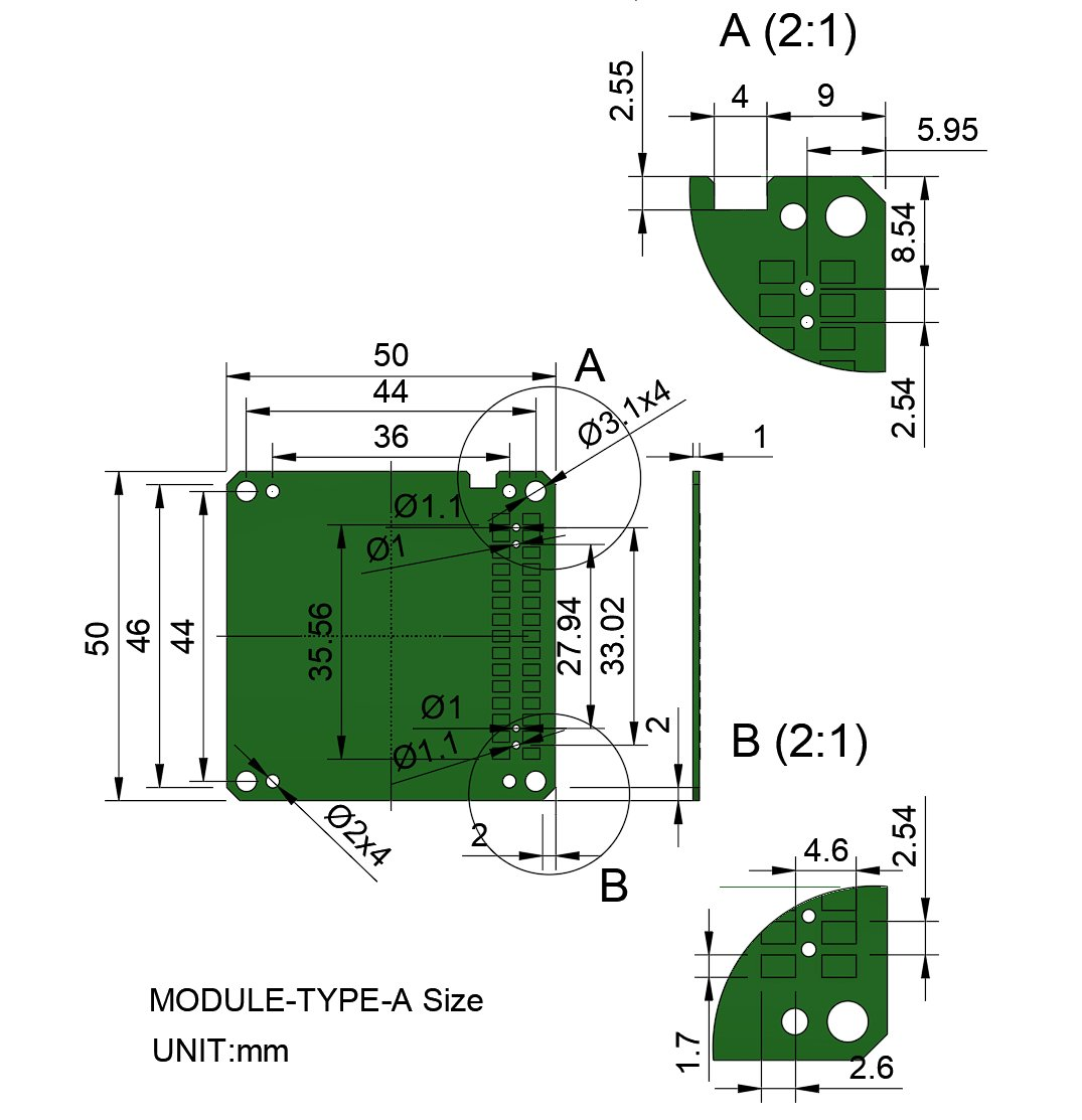
Ports placement
From the attached figure, you can see that there are already two limitations regarding the position of ports and headers:
- on the right side, the M-Bus (can't see that from the picture actually, but you can check M5Stack docs) takes up most of the available board outline
- on the bottom side you have the keyboard
You can see the general outline of the board from the picture below.
So I ended up placing the ports I was most interested in to the left and top side of the PCB.
In particular,
- I've placed the USB port to the left to be consistent with the charging port of the M5Stack and to not have awkward pulling forces on the same side as the antenna connector;
- Buttons were also placed on the left side so you can reach them easily with your fingers (for right handed folks at least) when holding the device, and LEDs close to them;
- Serial port and SWD ports are both at the top. Could have been placed on the left side as well but I had no more place for that.
Discussions
Become a Hackaday.io Member
Create an account to leave a comment. Already have an account? Log In.