 Bud Bennett
I've been simulating the daughter board voltage regulators lately. It seems like the data sheets for these LDO regulators, and the switchers too, don't account for any inductance in the power input leads. That's not the case here. I expect almost all users (except maybe some that employ batteries for power) are going to have relatively long -- around 1 meter -- leads running from the power adapter. This creates both lead inductance and mutual inductance between the leads if they are close together.
The lead inductance depends upon the diameter of the wire and its length. The mutual inductance depends upon the distance between the two wires. All of this can be modeled in SPICE.

It is not too difficult to create a model for the input power leads that depends upon the wire's AWG and length. The coupling between the wires depends upon their separation, which is pretty small for these thin wires, and therefore K is at the high end of the range (between 0.7 and 0.9) I believe. The interesting thing to note is that the higher/thinner AWG tends to have a higher inductance, but also a higher resistance that tends to lower the Q of the tuned circuit. For example, a 1m long 26AWG wire has an self inductance of 1.68µH and R=128mΩ, where the same length of 30AWG has a self inductance of 1.78µH and R=327mΩ.
I first discovered this when I simulated the LP2951 LDO. The data sheet shows a pretty basic application:

A minimal input bypass cap and 2.2uF for the output. And this is what the data sheet has to say about bypassing:
A bypass capacitor is recommended across the
LP2950/LP2951 input to ground if more than 4 inches of
wire connects the input to either a battery or power supply
filter capacitor.
Input capacitance at the LP2951 Feedback Pin 7 can
create a pole, causing instability if high value external
resistors are used to set the output voltage. Adding a 100 pF
capacitor between the Output Pin 1 and the Feedback Pin 7
and increasing the output filter capacitor to at least 3.3 F
will stabilize the feedback loop.
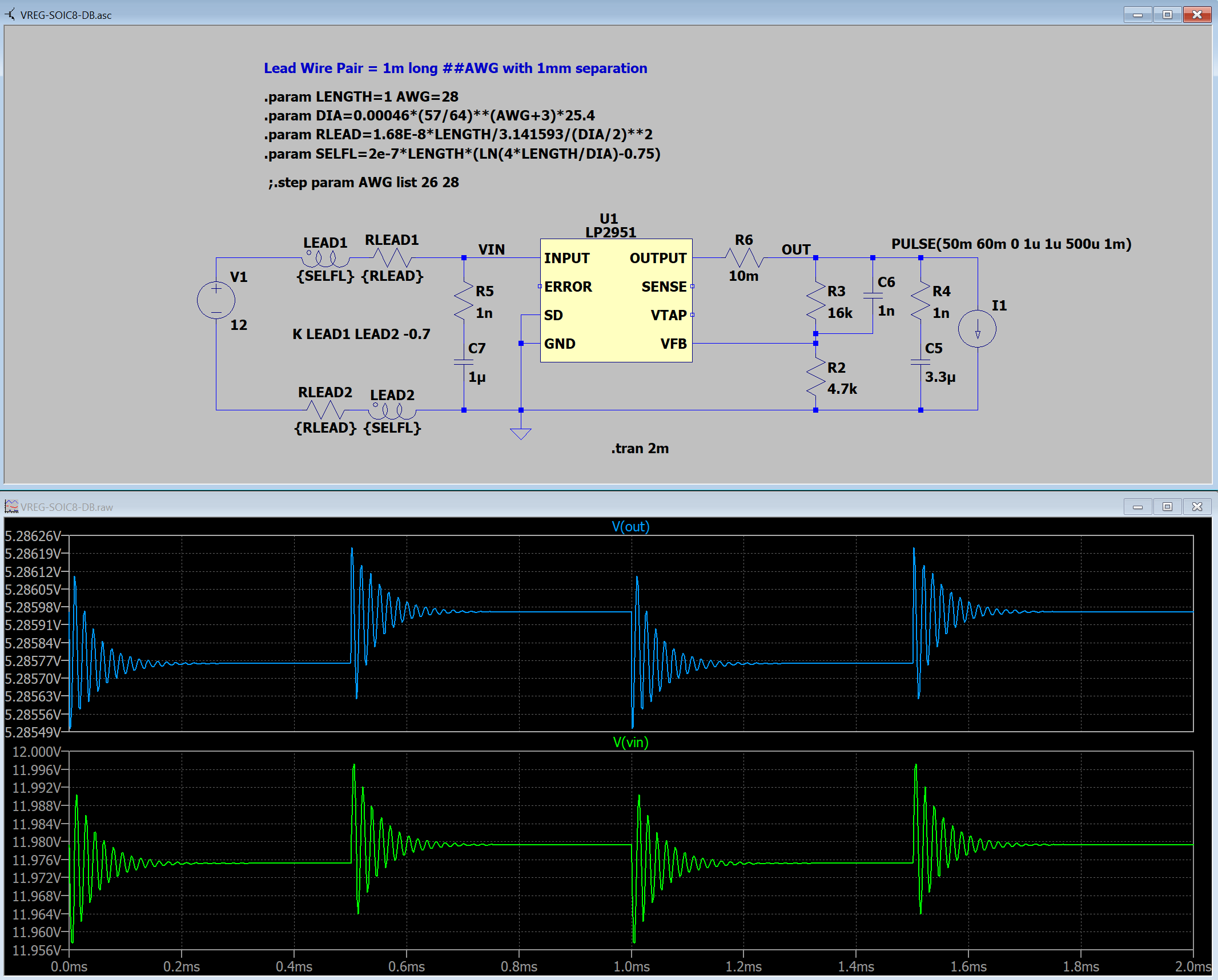
So this is the simulation result when I used the suggested values for ceramic capacitors, 1uF at input and 3.3uF at output, and set the length of the input leads to 125mm (~5in) and AWG=28: (load current is 50mA)

That doesn't look too good. The data sheet specifically states that low ESR bypass caps can be used. This is presented in a plot:
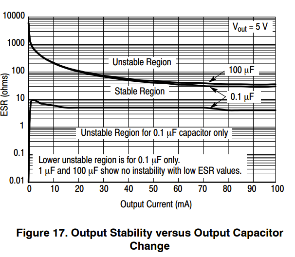
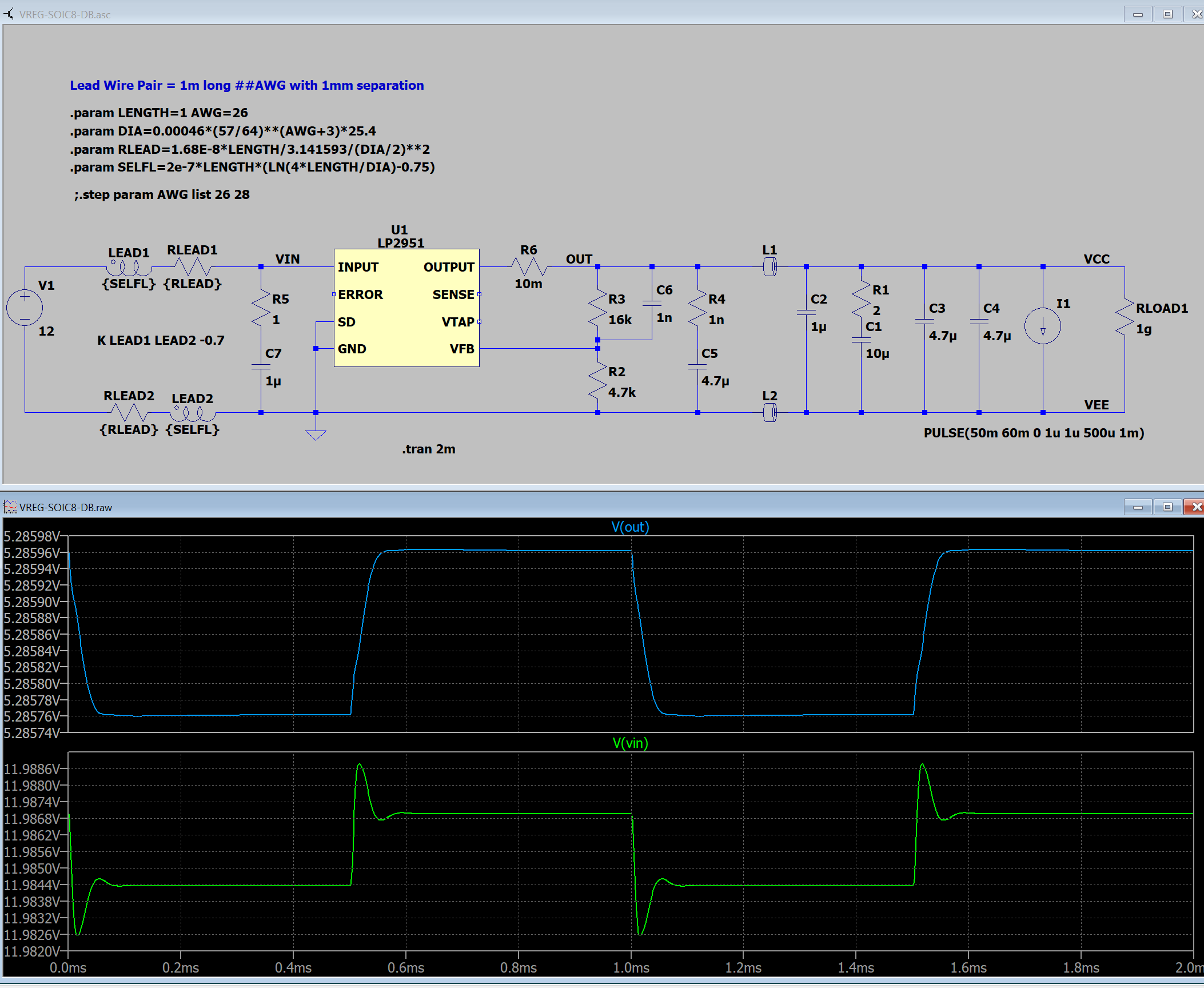
If I set the length of the input leads to 1m the oscillation disappears for steady state (due to the lower Q), but still looks pretty ringy dingy when excited:
In order to kill any possibility of oscillation a 1Ω snubber resistor should be added to the input capacitor. Then things look pretty good, even when driving the inductive looking load of the slim probe.
That underdamped response is due to the ferrite bead inductance and doesn't go away with increased snubber resistance. There apparently is no need for any large ESR output capacitor, but I will keep a discrete resistor in series with the output capacitor just in case.
Mutual Inductance Effects on the Buck Converter Daughter Board Design:
After all of that prior discussion, I won't bore with the details here. The problem I have is that I was not able to simulate the buck converter (off-brand manufacturer with limited modeling resources) and released the design without adding any discrete snubber resistors.
I fudged a simulation by using a similar switching converter IC model that ADI had a model for: the LT1616. As expected, the buck converter did not like the inductance of the input leads either. But it appears that the snubber resistors might not be necessary. The only way to tell is to build it and test it.
I put the lead inductance model in series with the buck converter input and checked in over various simulation parameters. There is one interesting phenomenon that show up: if you connect a powered adapter to the daughter board there's a chance that you can damage the daughter board. Here's one case where having cheap 30AWG leads from the adapter can save you. I ran a simulation of this event using 26-30AWG lead wires. Here is the result (without a snubber at the input):
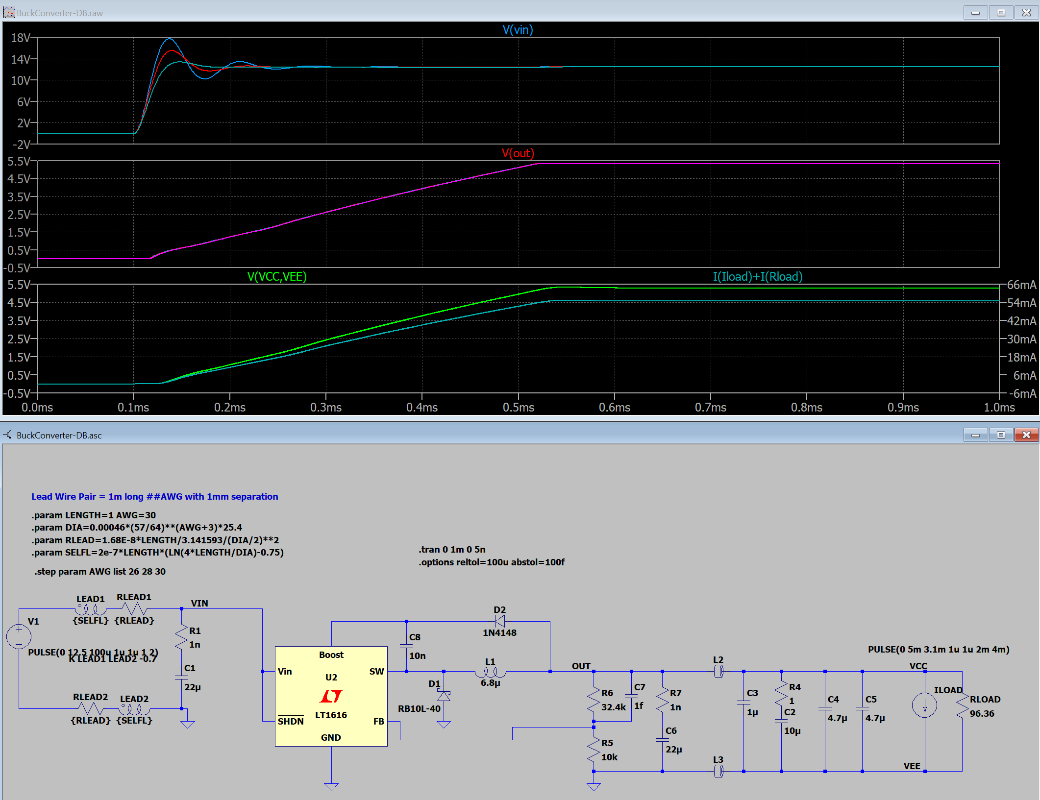
The smaller AWG wire doesn't produce as large of input spike because the higher wire resistance de-Qs the L-C tuned circuit at the input. The way to avoid this scenario is to solder the adapter lead wires to the daughter board -- the rising voltage waveform will be much slower. Otherwise, even a 0.5 Ohm snubber resistor in series with C1 will do the job.
Discussions
Become a Hackaday.io Member
Create an account to leave a comment. Already have an account? Log In.