 Bud Bennett
I really didn't need to modify the probe for performance issues. This last revision was to allow for two footprints of the trimmer capacitors. I found a cheaper version of the trimmer cap -- SCG3S300 8-30pF, for less than $1/each. The JR300 is slightly smaller, but breaks the bank at nearly $5/each. The other change that I made was to parallel the input capacitor string with the input resistor string. That way the capacitors don't float, which kind of bothered me a bit.
I left C11 and C12 unpopulated and used 300pF and 270pF for C9/C13. This combination was too high and I couldn't compensate the probe. I replaced C13 with a 220pF, which then required C11 to be 47pF to get the attenuator in the range where C15 could compensate. I used a different compensation method, which I will describe fully in another log posting. I powered the probe with a buck converter daughter board using a NEX40400 converter and fed that with a USB trigger board set to output 9VDC.
Supply current with 5.3VDC applied -- 55mA.
Here are some measurement of this latest version:
- CMRR @30Hz = -82.5dB (1.5mVpp/20Vpp)
- CMRR @ 1MHz = -74dB (1mVpp/5Vpp)
- CMRR @ 10MHz = -60dB (5mVpp/5Vpp)
- CMRR @ 20MHz = -52dB (13mVpp/5Vpp)
- CMRR @ 40MHz = -44.4dB (30mVpp/5Vpp)
These measurement use output voltage/input common mode voltage.
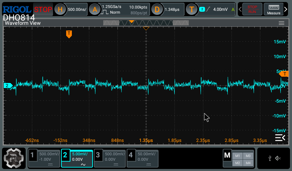
All of the measurements are using 100mm flying leads with 220 Ohm series resistors. Here's a scope trace of the probe hooked to the scope's calibration signal:
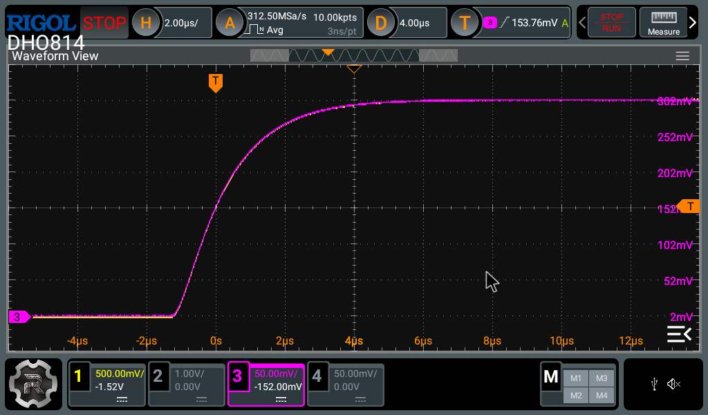
It is overlaid CH1 and very nearly identical (but noisier.)
I now have a signal generator, so I can take reasonable measurements to 60MHz. I found that this is trickier than it seems. Any amount of lead inductance will change the result. After several attempts, I eventually followed Paul's approach and soldered a 51 Ohm resistor between the center contact and GND post of a spare female SMA connector as shown below:
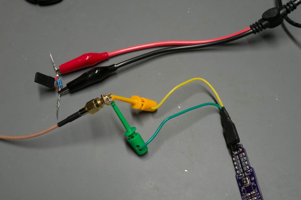
The leads that came with the signal generator caused some weird effects that disappeared (mostly) when I switched to the leadless version. This is what I measured with the probe connected to the 1Meg/15pF scope input with a 30cm coax pigtail.
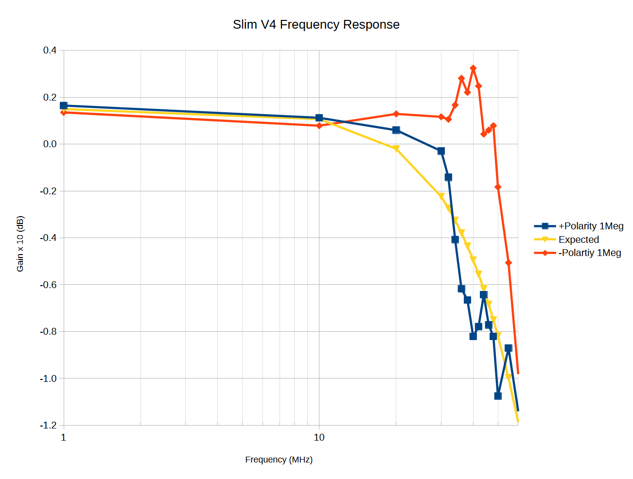
It's really not as bad as it appears. I plotted an ideal response in yellow for comparison -- using a 51 Ohm termination resistor at the generator output increases the gain by 0.17dB. Remember, a 1 dB drop is less than 10%. It's basically flat until 30MHz. What is odd is that the response of the positive signal path is different than the negative path. The negative path peaks slightly between 30-50MHz and the positive path dips a corresponding amount. I can't explain this, but it is not a huge effect. I suspect that most of it is reflections from an unterminated line into the scope, but the probe is designed for a 1Meg scope input. I performed similar measurements with 50 Ohm terminations at the scope input (with lower signal levels) without any significant change in the result. I also did not see any significant difference between using 100mm flying leads and a very short (~10mm) Dupont connector directly across the signal generator load.
V3 Buck Converter Daughter Board Evaluation:
The purpose of this V3 revision was to add a capability to prevent the switcher from operating until the input voltage is above roughly 6V. The thought is to prevent power applied to the probe when a non-PD compliant adapter is connected and only generates 5VDC. I plan to eventually test at least six buck converter boards populated with different components. To demonstrate that the PCB works I just tested two: NEX40400B IC and the AP64060Q IC. Both converter IC are synchronous switchers that operate at 2.2MHz.
I did not record detailed data, but did get some good results.
The NEX40400B:
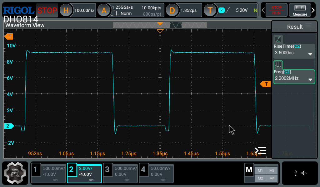
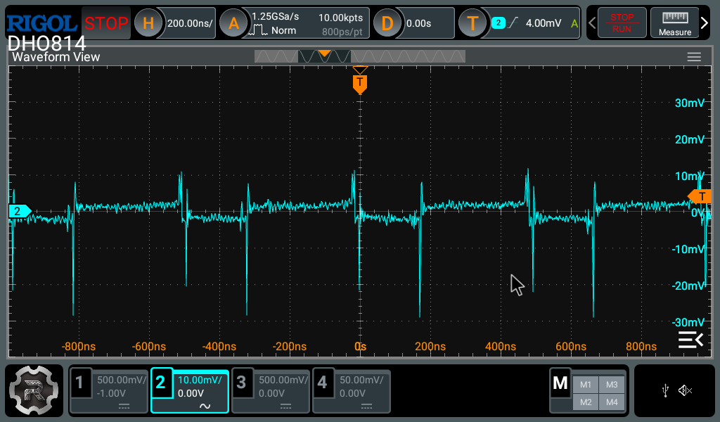
This switcher is forced PWM -- that's what the "B" stands for. I didn't think there would be any good reason to have the converter change modes for improved efficiency give that the probe pretty much consumes a constant load current. Used a Sunlord SPH2016 10uH inductor. Under the active load the converter had pretty poor load regulation, dropping from 5.34VDC with no load to less than 5.3VDC with a 70mA load current. It's line regulation was excellent -- less than 2mV change from 7V to 12V applied input voltage. I took scope traces of the switching node and the output ripple voltage. Both were excellent.
Lastly, I checked to see if the converter would prevent operation if the input voltage was too low. The converter did not generate any output voltage when the input voltage was below 6.7VDC. There is considerable hysteresis -- the input voltage has to drop below about 6V before the converter shuts off, which is still acceptable.
The AP64060Q:
I used a different inductor -- Suntech SLW2016 10uH. This converter IC can change its UVLO voltage using a single resistor connected to its EN input. A 2.2Meg resistor sets the UVLO above 6V -- and it works. The line and load responses were both excellent -- less than 2mV change over expected line and load variations. Here's what the switch node and output ripple voltage look like:
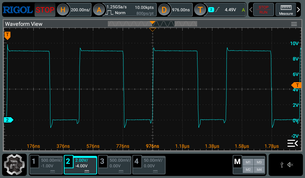
The switch node looks very good, but there's quite a bit more spike transients at the output than the NEX40400B.
Discussions
Become a Hackaday.io Member
Create an account to leave a comment. Already have an account? Log In.