 Bud Bennett
At this point your 100MHz probe is done...except for placing those two last components, C11/C12. Here's what you need to do. If the probe is working then connect the inputs to a suitable square wave source with at least one reasonably fast edge -- a rise/fall time between 100ns-300ns. If it is too fast you might get artifacts from the parasitics in the attenuator. Too slow and you will not be able to determine proper values for the C11/12. I recommend the following circuit, which connects to my 3Vpp/1kHz scope calibration output.
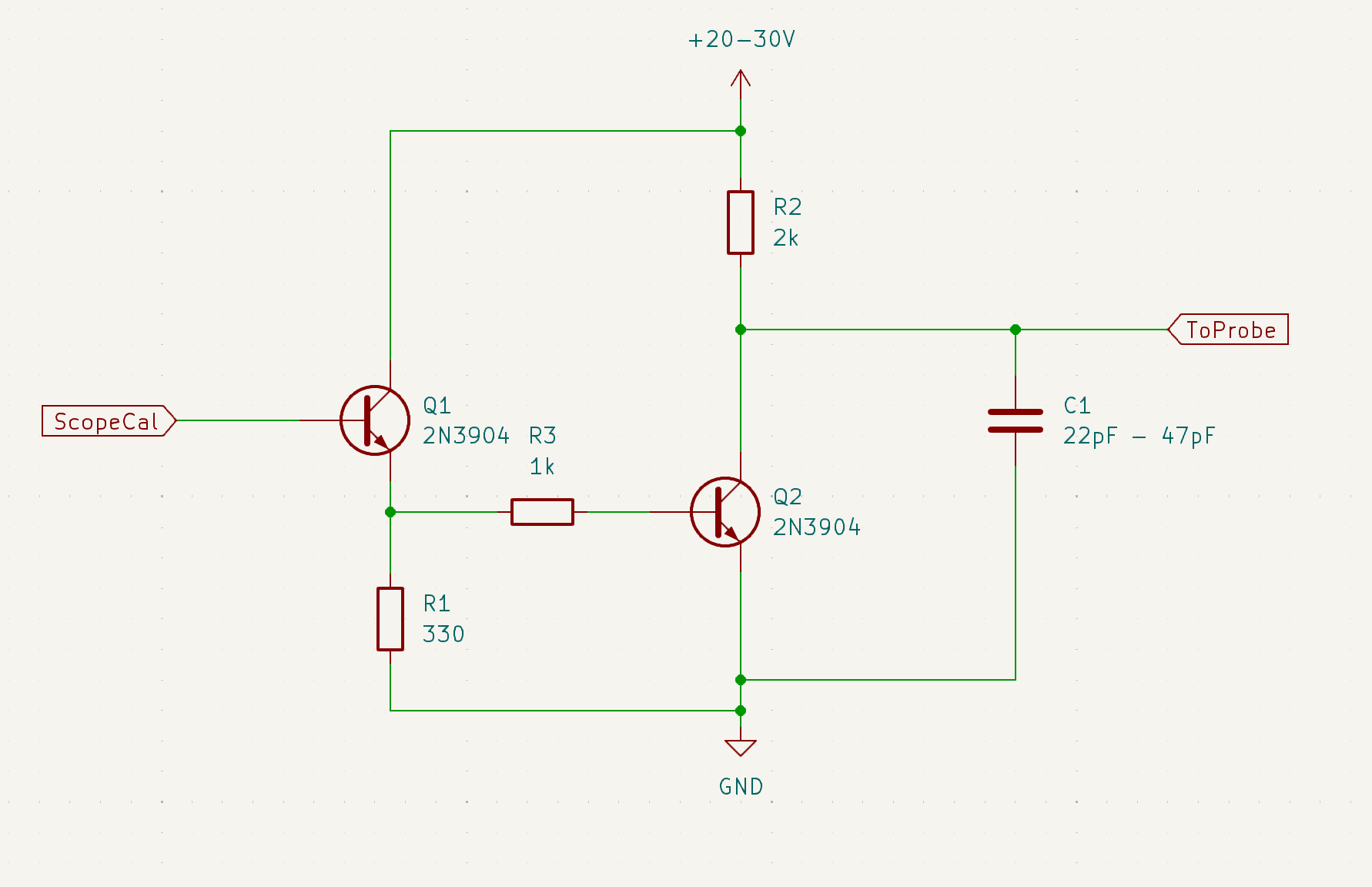
The two 2N3904 BJTs should be easily available, if not already in your kit. You might not need C1, depending upon what medium you use to construct the circuit. It should not be very sensitive to wiring mess ( so just use a plastic proto board.) If you drive it with the scope calibration output the rise time is nearly 300ns. If you drive it with a reasonably fast (<20ns fall time) square wave the rise time is about 150ns. If you hang a nominal 10x scope probe at the output the probe's capacitance will make the risetime slower -- so don't do that.
It is also recommended that only the rising edge be used to compensate the diff probe. The falling edge is not constrained.
Step Number 1 -- Calibrate the DC CMRR:
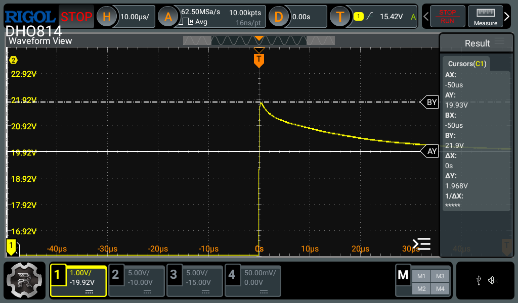
Connect both probe inputs to your square wave source output. You should see something like this:
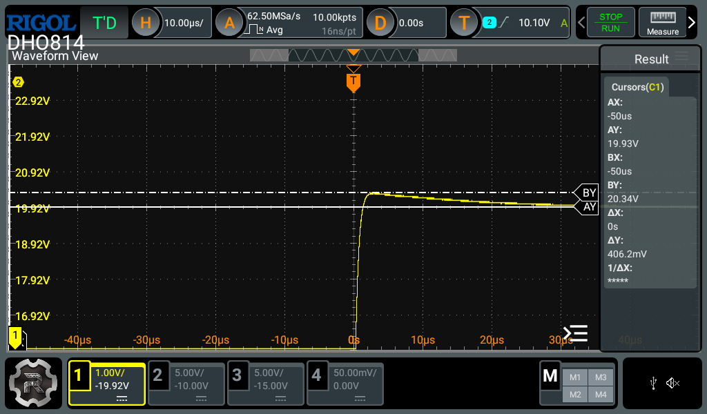
Adjust RV1 until the steps are matched. You can ignore the spikes at this point. It is important to match the final voltage values. As so:

Step Number 2 -- Calibrate DC Offset:
Now adjust RV2 until the probe's output offset voltage is removed. If you don't trust your scope's DC levels to be accurate then just connect both of the probe's inputs to the scope's GND and use a DVM. Here's what it should look like when you are probably close enough:
Remember the scope is multiplying the probe output by 10, so this offset reading is well below 1mV. At this level my probe output jumps around a bit, probably due to popcorn noise (1/f noise).
Step Number 3 -- Calculate the Values for C11 and C12:
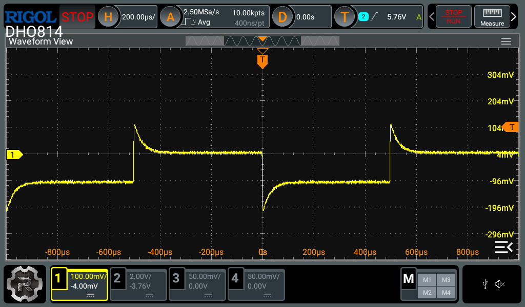
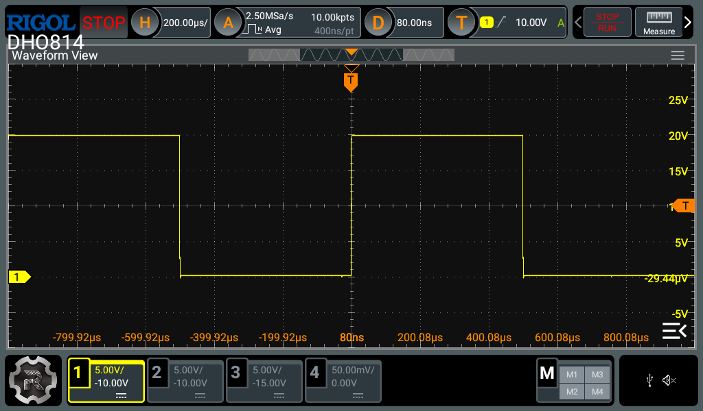
Here's what a 100MHz probe produced when connected to custom calibration signal:
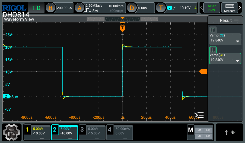
Use 20Vpp for this test. Channel 1 is the diff probe output (10x) and Channel 2 is a compensated 10x passive probe connected to the same output. The peaks show that the probe's capacitive attenuator doesn't have enough capacitance in its lower leg (i.e. the AC gain is too high), and therefore the signal overshoots a bit and then settles to the value that the resistor attenuator thinks is correct. Channel 2 is just there for a sanity check (that you believe me). I have the scope measuring a swing of 19.84V on the probe output.
Compensating the Positive Signal Path:
You need to measure the overshoot of the square wave signal and figure out how much additional capacitance must be added to the attenuator to make the DC and AC attenuators match. (If your signal is rounded instead of peaked, then you are screwed...the 0805 capacitors are too large and one of them must be replaced with a smaller value.)
Set the trigger for a 10V level (of course this depends upon your scope calibration square wave, or whatever square wave signal you are using now.) The more vertical sensitivity you have the better your measurements will be, but don't overload the scope input to much if you suspect it is becoming distorted. For this example, I'm using 1V/div, with signal averaging set to 32 -- your trigger needs to be rock solid with this amount of averaging.
Adjust the trimmer capacitor, C15, to yield the maximum peak voltage. This will be the minimum capacitance that the trimmer can produce. Measure this peak value. Then adjust the trimmer capacitor to yield the minimum peak value. This is the maximum trimmer capacitance. I used a metal tool to adjust the trimmer cap. When I remove the tool the peaks relax upward. Use your best judgement as to where the minimum and maximum trim points are.
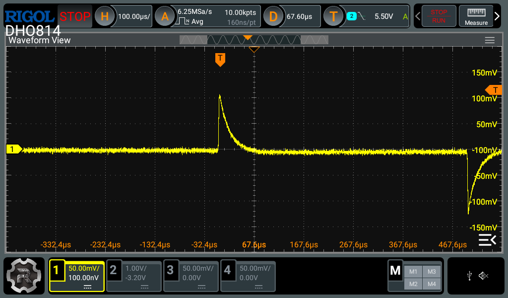
The difference between these two peaks is what the trimmer capacitor can produce. If I want the trimmer range be centered around the flat square wave response, I need to select a tuning capacitor that puts the capacitive attenuator in the center of the trim range of the trimmer cap.
The average overshoot voltage is 1.187V. Therefore the attenuator capacitance of the lower leg is almost 6% below what is needed to center the trim range. (I'm being lazy here, but it's close.) We must take into account all of the capacitances that occupy the lower leg of the attenuator, for which we really don't know those exact values. But here goes in my case: 330pF + 220pF + 20pF (trim cap nominal mid-range -- could be larger) + 3pF parasitic capacitance (due to diodes and opamp input capacitance) ~ about 573pF. So it appears that I need to increase the lower leg of the attenuator capacitance by about 35pF (0.06 * 573pF = 34.4pF). There is some peril is using these numbers because we don't really know what the capacitor values really are (but they should be somewhat close if using 1% tolerances, so let's proceed.)
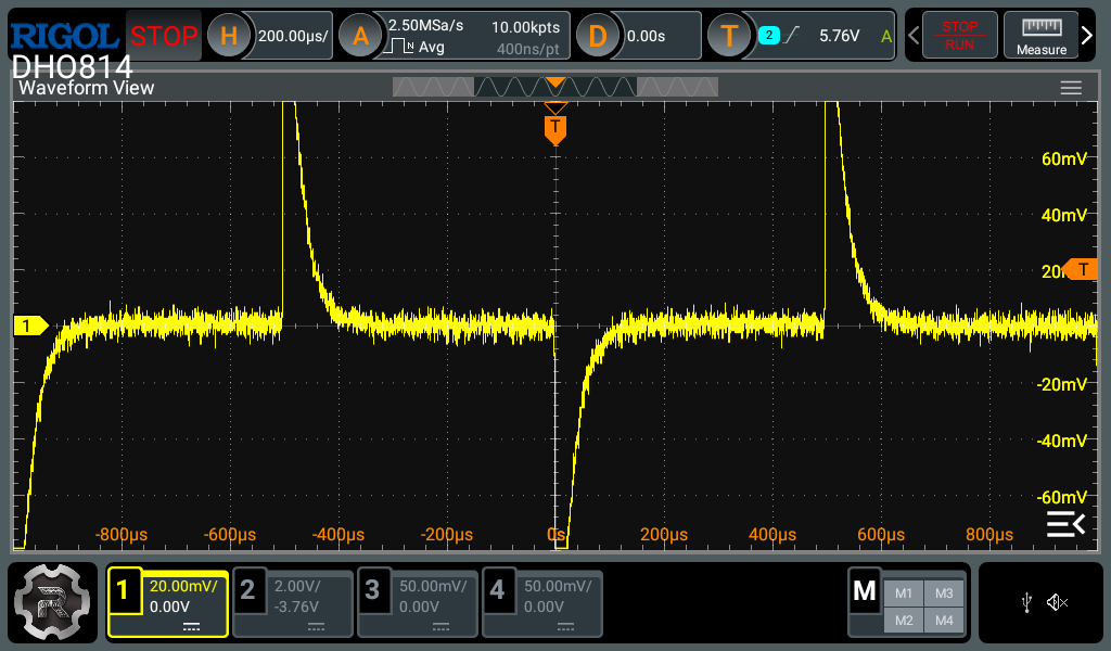
I dug out a 0603 39pF NP0 cap from my inventory and solder that in C11's place. Here's the result, after trimming for flatness:
That's pretty flat! (Ignore the spike on the trailing edge because the drive circuit isn't very good in that direction...don't ask.)
Flip the probe leads on your square wave source so that the positive probe lead is attached to GND and the negative probe lead is attached to the source. Go through the same steps that you did previously to determine the value of C12. Remember that only only the rising edge (of the input) is useful for calibration.
Step Number 4 -- Compensating the Negative Signal Path to Match the Positive Signal Path:
I'm going to propose a different method to compensate the negative signal path of the probe. The previous method was to just flatten the square wave output of the probe and call it good. That approach may not deliver a good CMRR result at higher frequencies. This new method will improve CMRR at frequencies below where the opamp CMRR dominates.
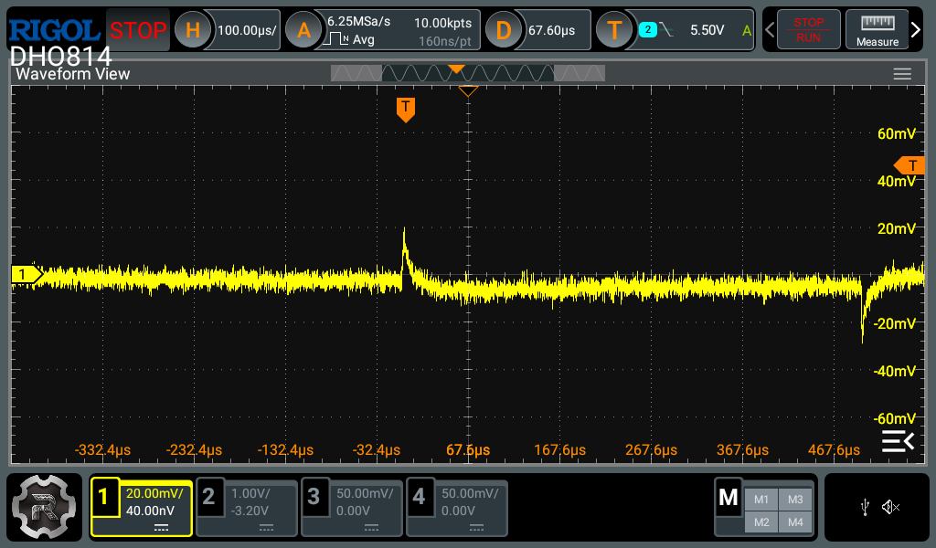
Find or make a signal source that can swing at least 20-30Vpp at 1kHz. Connect both probe leads to the same signal source output. You will get an output from the probe that looks like this:
Adjust the NEGATIVE PATH trimmer, C16, until the spikes are minimized or disappear entirely. What this last step does is match the AC gain in the negative signal path to the AC gain of the positive signal path. It will probably not be possible to eliminate the peaks. This was my best result (the point where I gave up.)
If you have a sinusoidal source you might be able to improve the CMRR. Connect both probe inputs to a 10kHz 20Vpp sine wave. Adjust C16 to minimize the amplitude of the probe output. You can also adjust C15 to minimize it even further. It won't require much adjustment. Here's what the probe outputs after I went through this process:
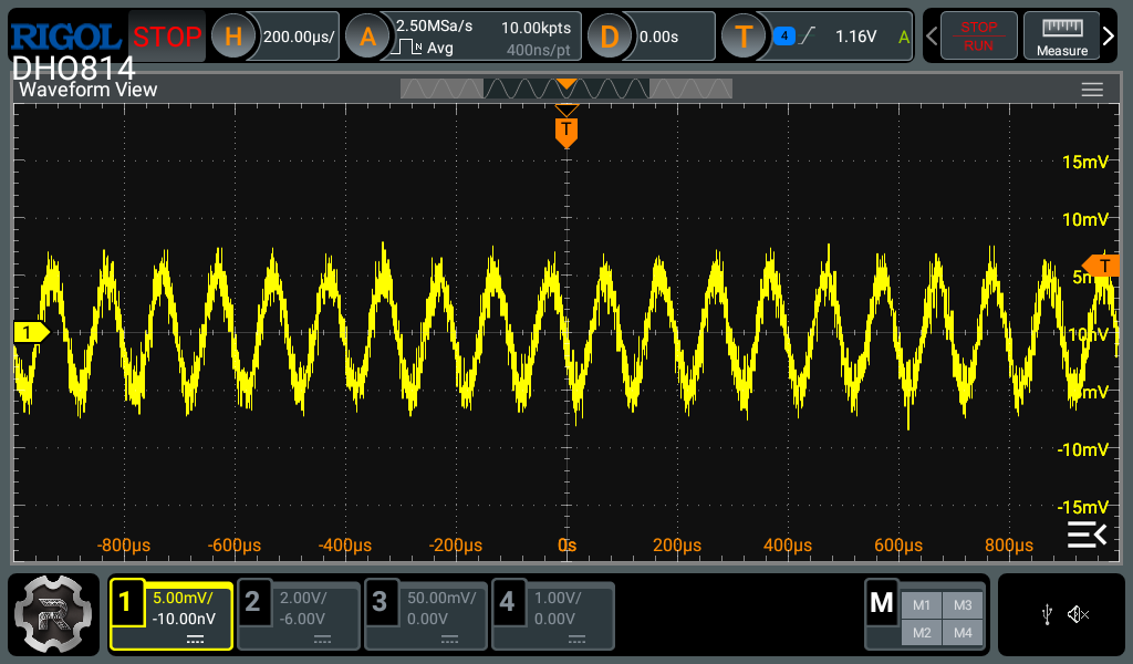
That's a 1mVpp swing at the probe output! So CMRR to a 20Vpp 10KHz sinewave is 86dB, or 66dB if it is input referred.
You can test this by switching to a sinusoid source and sweeping its frequency to around 10% of the probe's bandwidth -- 10MHz for the 100MHz probe. If you compensated the probe properly the output of the probe should stay small (CMRR < -50dB) over the entire frequency range.
If you put the probe in a case you will need to repeat the compensation process. The probe should be powered for at least 15 minutes to arrive at a stable temperature within the case.
Now you're done.
Discussions
Become a Hackaday.io Member
Create an account to leave a comment. Already have an account? Log In.