 kooksay
I submitted the V1 of the power board to the factory for PCB fabrication. Although it will still take a few days before I receive the board, I’ve already started working on the adjustments.
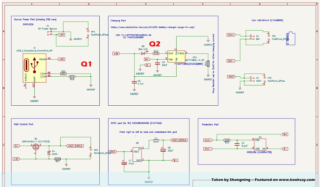
In the initial design, there didn’t include TVS protection for the Type-C connector, since I wanted to quickly verify the core functions. But today, I’ve added that section — it’s actually quite simple, requiring only a single TVS diode.
To make hand soldering easier, I avoided the commonly used ESDA25P35-1U1M due to its packaging being unfriendly for manual soldering. Instead, I chose the SMF5.0CA, which has a large enough footprint to make hand soldering more convenient.
As for the LED indicators, they’re relatively more complex. That’s because the charging chip I’m using, the MCP73831-2, only provides a single STAT pin. The typical application diagram from the datasheet shows only one indicator LED. Fortunately, this pin can output three different states — LOW, HIGH, and HIGH-Z — which makes it feasible to drive two indicator LEDs.
In the modified circuit, I’ve used a bi-color LED package (one housing both red and green LEDs), along with a logic gate circuit. This allows the red LED to light up during charging, and the green LED to light up once charging is complete.
I won’t be show the related schematics for now, as I prefer to wait until I receive and test the V1 board. After identifying any issues and making the necessary adjustments and improvements, I will then release the complete V2 circuit for the button cell charging section.
Below is the schematic diagram of Version 1, with two areas marked in red that are either in need of improvement or currently being improved.
Discussions
Become a Hackaday.io Member
Create an account to leave a comment. Already have an account? Log In.