 Arnov Sharma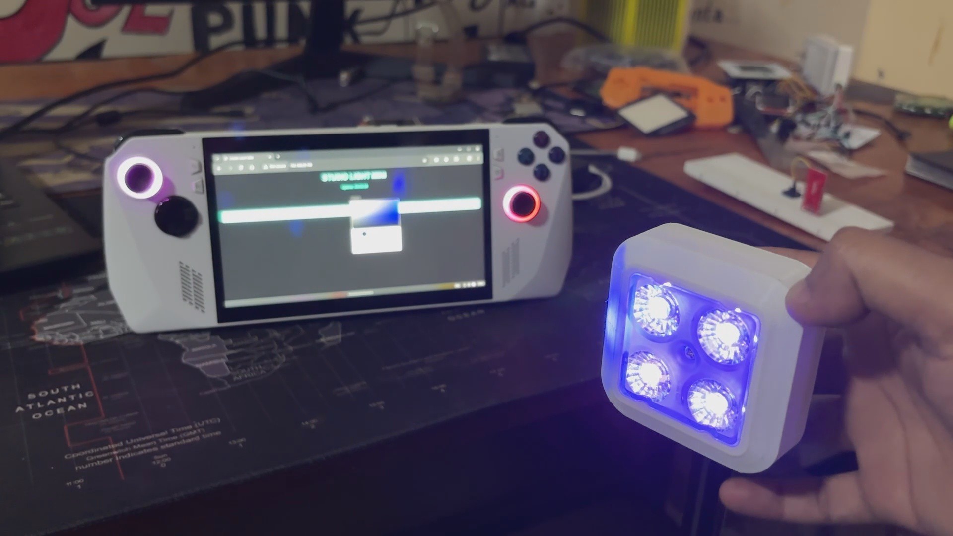
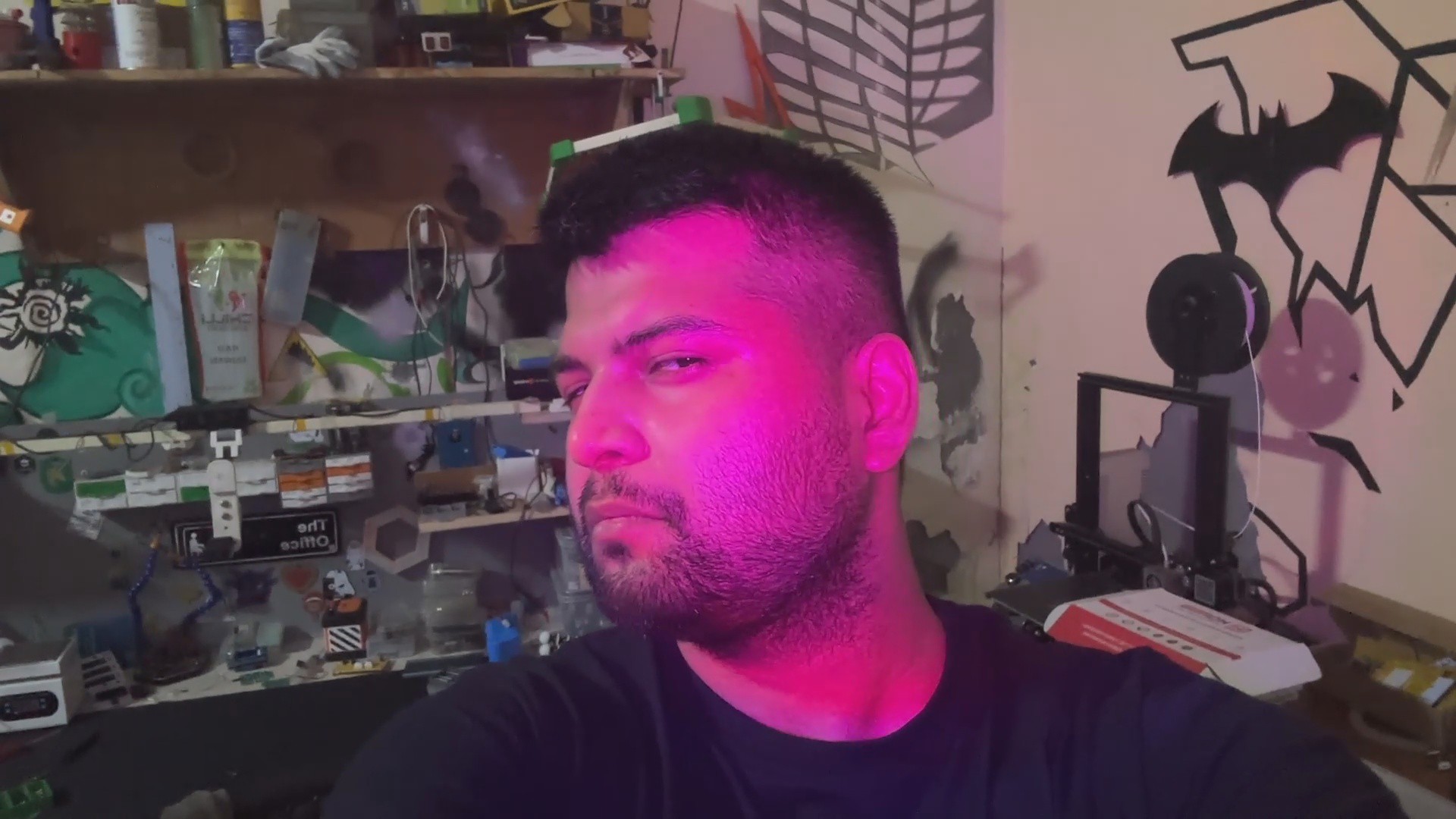

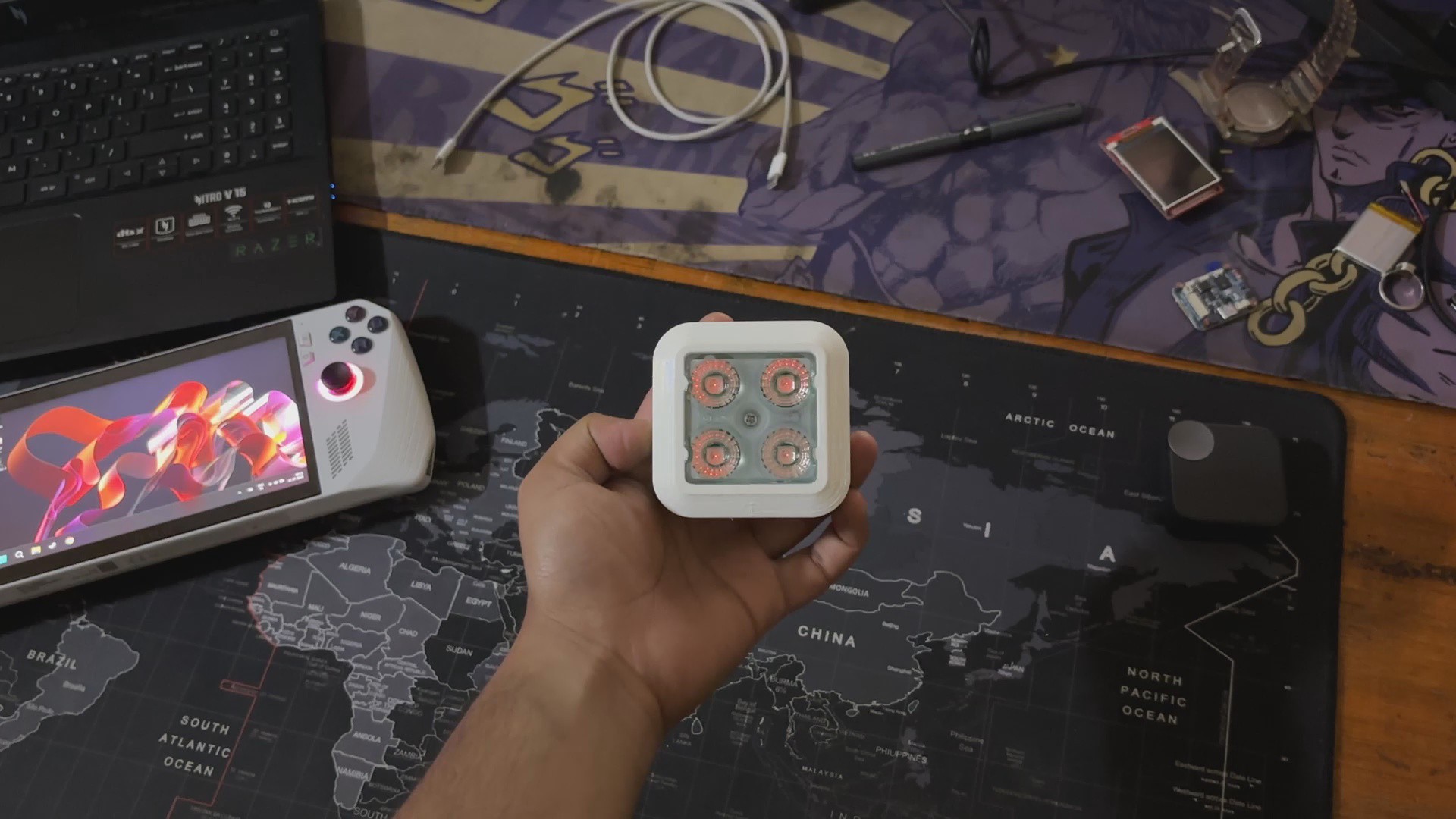
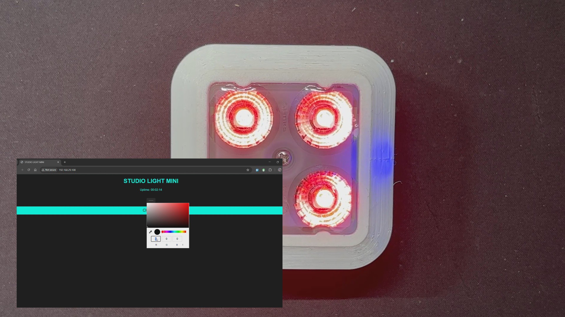
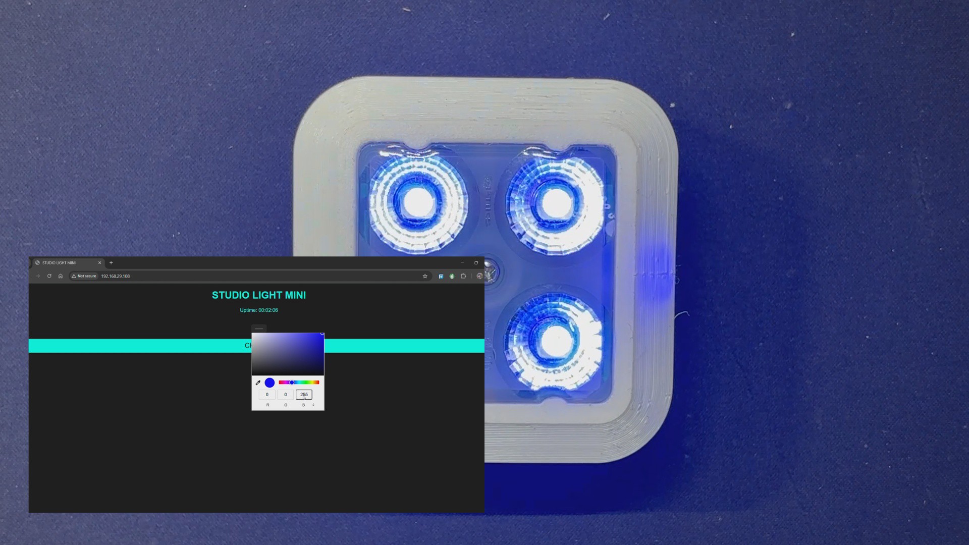
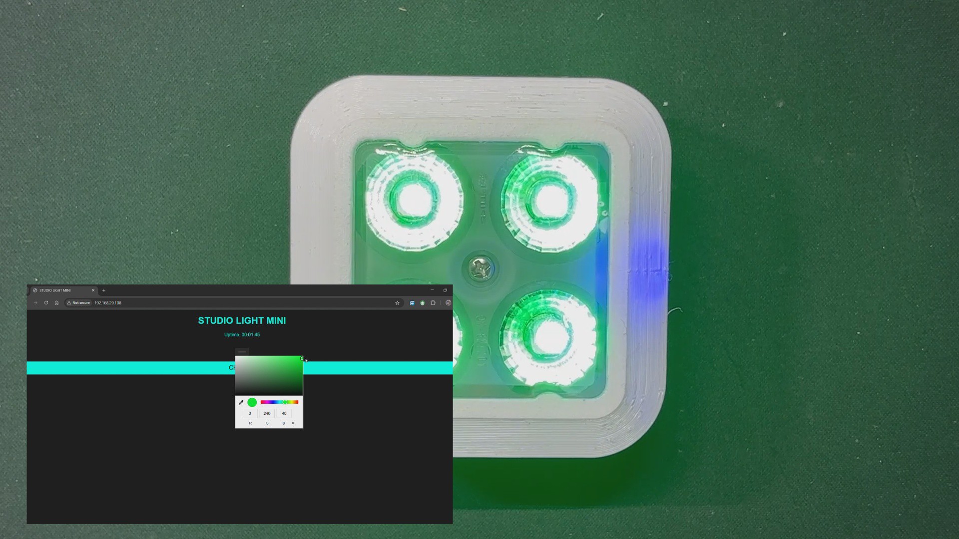
The Studio light, powered by an ESP8266 microcontroller, links smoothly to a browser-based web app, allowing for exact color choices and dynamic control directly from your phone or laptop.
The Portable Studio Light was created to address an actual problem: I just relocated and found myself frequently hopping between two workplaces. I needed a lighting setup that was portable, easy to mount anyplace, and strong enough to enhance my video output.
Our Setup is powered by an ESP8266, with a custom 3D-printed lens and enclosure to make the most of only four WS2812B LEDs. The web app is where the magic happens: it's simple, responsive, and works on any device. I've used my phone, laptop, and ROG Ally to control it. Simply select a hue and it refreshes instantaneously, allowing us complete creative freedom no matter where I am working.
Previous Build


previously, I created a similar Studio light that was far bigger and more powerful in terms of both light and battery capacity. In the initial version, I used two PCBs connected by a 3D printed bracket and a long PCB standoff. The two PCBs consisted of an LED board and a control board. The LED board contains all of the non-addressable SMD RGB 5050 LEDs, including Warm White and Cool White LEDs.
The Control board included a PICO 2 with a display, a few buttons, an integrated power source, and two 8205S Mosfets as a switch setup that we linked to the LED board to turn on and off the Warm and Cool white LEDs.
One major issue with the project was its size, and I chose to use the WS2811 chip instead of an RGB addressable LED. I connected more than ten LEDs in parallel with the WS2811 IC, but the maximum current the WS2811 can sustain is roughly 20 mA per channel, causing all LEDs to flash very dimly in all R G and B modes.
The new portable version resolved the current issue by replacing the WS2811 IC with higher-quality WS2812B LEDs.
You can check out the previous project from here—
https://www.hackster.io/Arnov_Sharma_makes/pico-studio-light-4eac11
3D Design

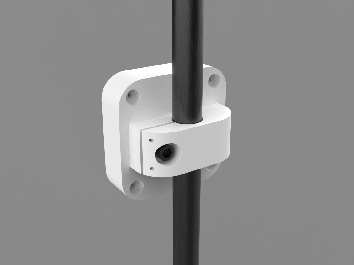
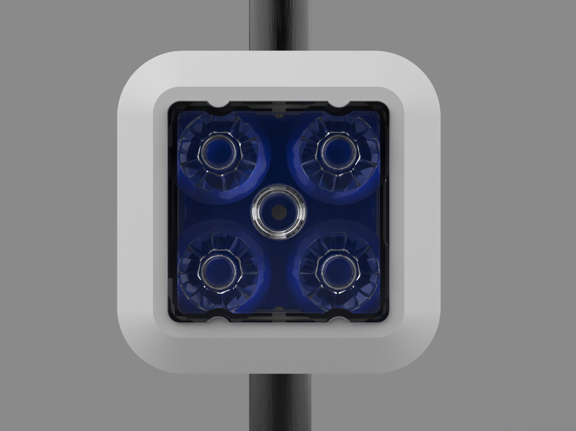
The 3D design of this project began with creating a proper-sized model of the lens that will be used in this build. The idea here was to place a PCB on the backside of the lens and then create an enclosure around it to house the batteries and electronics. The entire device will have a Stand Holder component that will be used to attach the device to any tripod or pipe.
The enclosure was designed in two halves: the front body and the lid section.
The front body has a huge opening in its center where the lens will be secured. The circuit was then modeled and connected to the lens, which is kept in place by a hole in the middle into which we will insert an M2.5 nut and bolt.
The lid is attached to the front body from the back and held in place with four M2 screws. The Lid Part also houses the Stand Holder Part.
We have created a 20mm DIA hole on the Stand Holder for attaching a tripod with this arrangement. We also constructed a slit and provided a hole and slot for installing an M6 nut and bolt; by tightening these nuts and bolts, the 20mm dia. hole size drops to 19.5 or less, allowing our device to be fastened securely with a tripod.
After preparing the 3D model, we exported the mesh files for all of the parts and 3D printed them on our K10 Max 3D printer with white Hyper PLA.
PCB Design


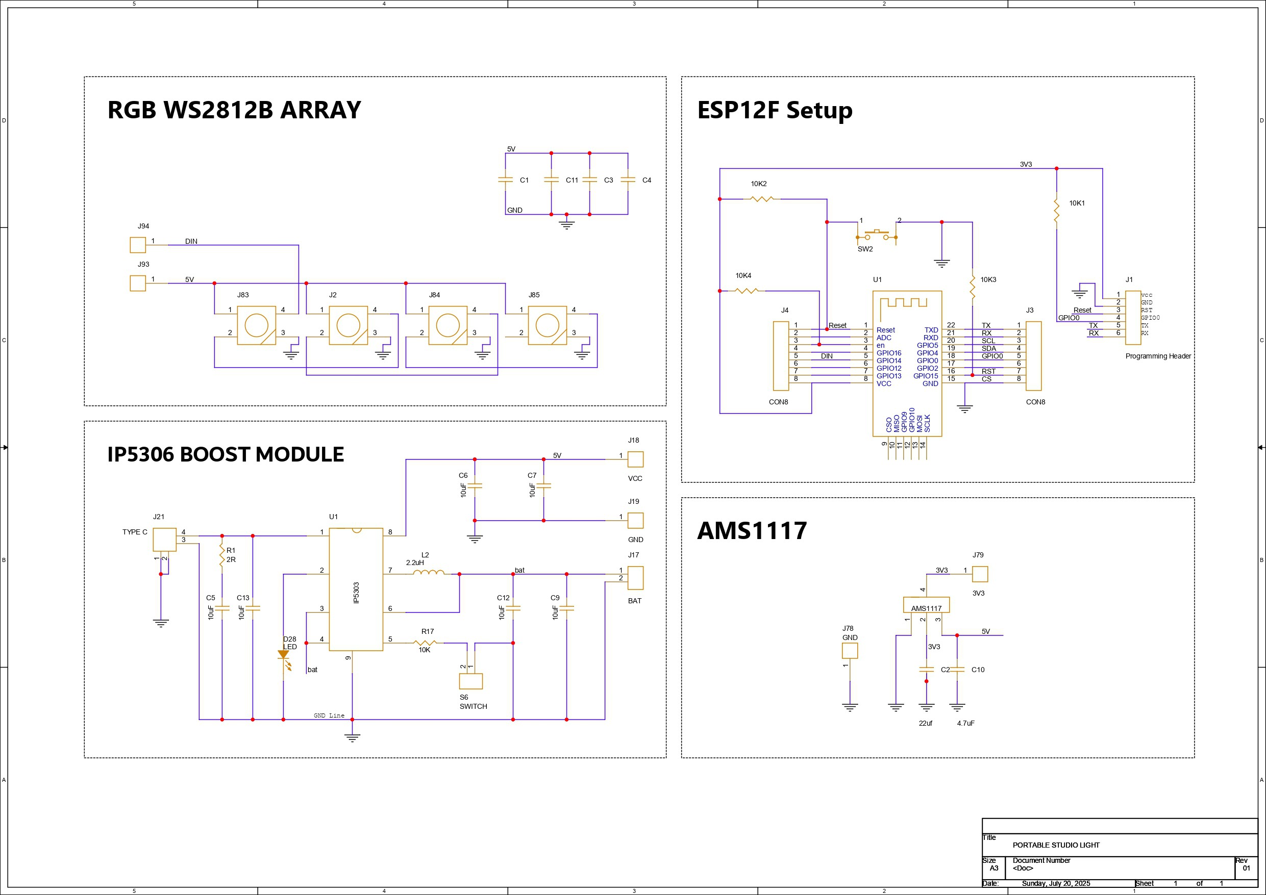
Let's have a look at the schematic for this project, which is divided into four primary parts, one of which is the microcontroller section, which in our case is the ESP12F setup. Here, we've connected the ESP12F module to a few 10K resistors in the minimal configuration required for the ESP12F to work. We also included a CON6 Header pin connector that connects to the TX, RX, GPIO 0, RESET, VCC, and GND pins of the ESP12F Module; this connector will be used to flash the ESP chip using a UART adapter.
Next, we have the Power source section, which is the IP5306 Power management IC Setup, which we have previously used in many of our battery-related projects. This SOIC8 Package IC can provide a stable 5V 2.4A from a 3.7V Lithium Ion or LIPO Cell and also includes many important functions such as overcharging protection, overdischarge, battery fuel level, and charging status.
Below is its datasheet if you want more info on this IC.
https://www.skytech.ir/DownLoad/File/2566_IP5306.pdf
Our ESP12F is a 3.3V device; however, the IP5306 provides 5V, which will easily destroy our ESP12F setup. To avoid this issue, we used an AMS1117 3.3V Voltage Regulator, which takes the 5V from the IP5306 IC and lowers it to 3.3V so that our ESP12F setup can function properly.
Finally, we have the RGB LED Array, which consists of four WS2812B LEDs linked together to make a four-chain addressable LED. We have also included four 100 nF decoupling capacitors, which will be placed near the VCC and GND pins of each SMD LED.
After finalizing the schematic, we prepared the PCB Design, which was really simple. We began by creating the board outline using a DWG file exported from our Fusion360 model, which we then used to construct the PCB outline in our PCB cad software. We placed all of the SMD components on the top side of the PCB except for the ESP12F module due to space constraints; all SMD components were extremely small and could easily be placed on the top side, but our ESP12F module occupied a larger area, so we had to move it to the bottom layer.
All of the through-hole components, including the Type C Port and Right angle Push button, were installed on the bottom side according to the mounting dimensions provided in the design. The mounting hole in the middle was also added by following the dimensions from the 3D model, as was the placement of RGB LEDs.
NextPCB PCB Service
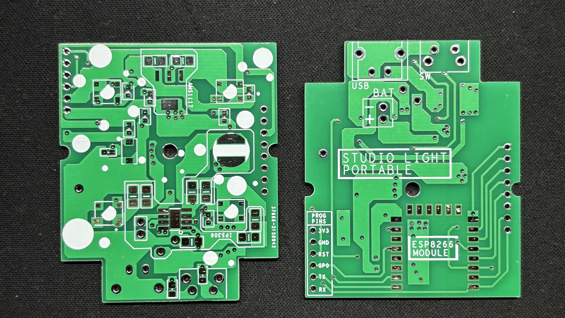
After completing the PCB Design, Gerber Data was sent to HQ NextPCB, and two orders were placed in a white solder mask with black silkscreen.
After placing the order, the PCBs were received within a week, and the PCB quality was pretty great.
In addition, I have to bring in HQDFM to you, which helped me a lot through many projects. Huaqiu’s in-house engineers developed the free Design for Manufacturing software, HQDFM, revolutionizing how PCB designers visualize and verify their designs.
Take advantage of NextPCB's Accelerator campaign and get 2 free assembled RP2040-based PCBs for your innovative projects.
https://www.nextpcb.com/blog/rp2040-free-pcba-prototypes-nextpcb-accelerator
This offer covers all costs, including logistics, making it easier and more affordable to bring your ideas to life. SMT services can be expensive, but NextPCB is here to help you overcome that hurdle. Simply share your relevant project, and they'll take care of the rest. Don't miss out on this amazing opportunity to advance your tech creations!
HQDFM: Free Online Gerber Viewer and DFM Analysis Tool
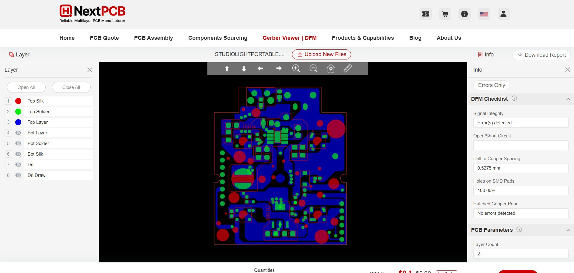
Also, NextPCB has its own Gerber Viewer and DFM analysis software.
Your designs are improved by their HQDFM software (DFM) services. Since I find it annoying to have to wait around for DFM reports from manufacturers, HQDFM is the most efficient method for performing a pre-event self-check.
This is what I see in the online Gerber Viewer. It's decent for a quick look, but not entirely clear. For full functionality—like detailed DFM analysis for PCBA—you’ll need to download the desktop software. The web version only offers a basic DFM report.
With comprehensive Design for Manufacture (DFM) analysis features, HQDFM is a free, sophisticated online PCB Gerber file viewer.
With over 15 years of industry experience, it offers valuable insights into advanced manufacturing processes. If you’re looking for reliable PCB services at a budget-friendly price, HQ NextPCB is definitely worth checking out.