 AranweLTT
Project description
The primary goal of this project is to create a standalone, paper‑programmable CPU that serves as an educational tool for teaching CPU architectures and assembly programming. At the same time, the CPU is sufficiently capable to support more sophisticated programs, which requires creative thinking to get the most out of the CPU's limited resources.
Achieving this calls for a careful balance between instruction set complexity and logic resource usage. On one hand, a reduced instruction set with a large memory allows complex routines through repeated simple operations (RISC approach). On the other hand, richer instructions can shrink program size when memory is limited (CISC approach). In a fully discrete implementation, both the number of logic chips and the size of program memory quickly balloon. By revisiting the TD4’s instruction encoding and overall architecture—eliminating wasted opcode bits and expanding operand flexibility—this design maximizes capability within a modest chip count and just 16 words of program memory.
Architecture
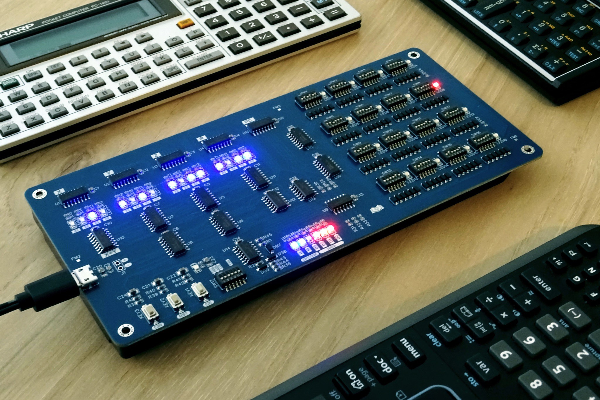
At its core, the CPU features four general‑purpose 4‑bit registers, doubling the TD4’s original count. Instructions are encoded in 6 bits: a 2‑bit opcode and 4 bits of operand/address data. Four primary operations are supported: immediate load into register X (LDX), register‑to‑register addition (ADD), conditional jumps on carry (JCC), and register moves (MOV). This concise set of instructions can be combined to implement loops, arithmetic routines, and complex control structures. Moving to a 6-bit instruction from the original 8-bit allows the use of single IC hex inverters and decoders, reducing chip count. It also reduces the ROM array board space all while keeping the same number of instructions and increasing register count.
Instruction set
| Mnemonic | Description | Opcode | Comment |
| LDX | Load value to register X | 00DDDD | X = DDDD |
| ADD | Add registers X and Y | 01SSDD | DD = X+Y |
| JCC | Jump if carry is clear | 10AAAA | PC = AAAA when carry = 0 |
| MOV | Copy one register to another | 11SSDD | DD = SS |
Each register is given a 2-bit address to designate it as a source (SS) or destination (DD) for a given operation. The addressing is as follows:
| Register | Address | Description |
| X | 00 | Input to adder, capable of immediate loads. |
| Y | 01 | Input to adder. |
| Z | 10 | General purpose. |
| R | 11 | General purpose, usually used as a Result register. |
Data path
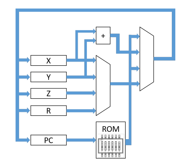
A distinctive aspect of the architecture is the use of multiplexers in place of a centralized data bus. Each register’s output is piped into a multiplexer used to select the source for write‑back, while a second multiplexer switches the common register input data between the adder, mux output or immediate data. Because every instruction completes in a single clock cycle, control logic is greatly simplified: the opcodes are decodes with a 1-in-4 decoder, and another decoder is used to select the destination register.
Control logic
Another uncommon design choice is the carry and jump logic. Usually the carry is a flag which is latched on an ALU operation. The flags is then typically cleared on a jump operation. But to keep the IC count down and the control logic simple, the carry is not latched and the jump logic is fully combinational. This has to be accounted for when programming: if the destination register of the add operation is different than the operands, then the carry remains valid after the add instruction, but will not be cleared unless the operands are updated.
Moreover, due to the lack of a non-conditional jump, it is possible to ensure the carry is clear and guarantee a jump is performed by either setting the x or y register to 0. It should be noted that the carry input is only passed to the adder on an add instruction, and will not be taken into account for a conditional jump. Hence if the carry input is enabled and an overflow by 1 occurs, a conditional jump with the same operands will consider the carry as being clear. A more detailed look of the control logic is shown by a Logisim simulation
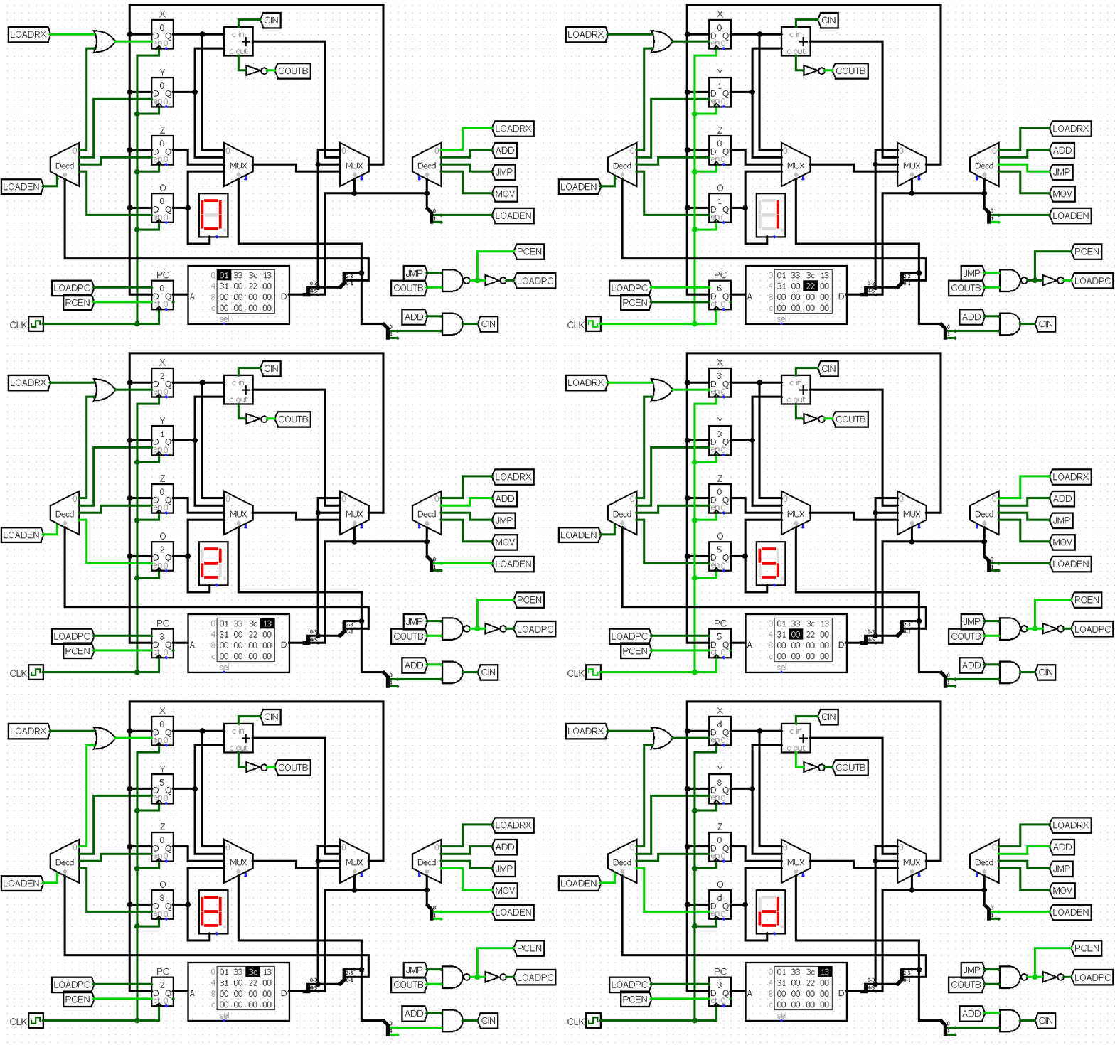
Note that this simulation is only identical in behavior, the actual gates making up the control logic are different because many signals are active high in Logisim while being active low for 74-series ICs.
Along with the Logisim simulation, a Python based assembler and simulator is available as demonstrated in the software examples section. It allows programming in assembly with support for comments and basic linker functions.
Example program
While the Fibonacci sequence is a very popular integer sequence, often visualized with a square spiral, a similar sequence exists but with a triangle spiral: the Padovan sequence (A000931). It is defined by the following recurrence relation:
The Perrin sequence (A001608) satisfies the same recurrence relations as the Padovan sequence, although it has different initial values. The first terms of the Padovan sequence are: 1, 1, 1, 2, 2, 3, 4, 5, 7, 9, 12, 16, 21, 28, 37, 49, 65, 86, 114, 151, 200, 265, 351, 465, 616, 816, 1081, 1432, 1897, 2513, 3329

(Spiral of equilateral triangles with side lengths which follow the Padovan sequence, Wikipedia)
For any integer n, the sequence of Padovan and Perrin numbers taken modulo m is periodic. The length of the period of this sequence is called the Pisano Period with the following first terms: 1, 7, 13, 14, 24, 91, 48, 28, 39, 168, 120, 182, 183, 336, 312, 56... (A104217)
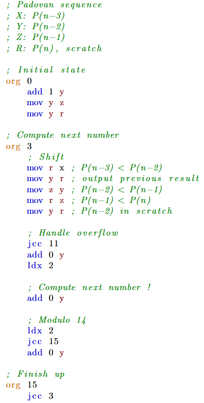
Within a 4-bit range (up to modulo 16), it is modulo 14 which is largest, with a period of 336. Sadly modulo 16 only has a period of 56, which would have offered a modulo 16 already with the 4-bit nature of the CPU. If this sequence modulo 14 were to be programmed on the board, a 336 4-bit number sequence will be generated while only having 16 words of ROM, showing this sequence is truly computed as it cannot simply be stored in the ROM.
Getting started!
Go over to the DIP74 Github repo and try to write a program generating an even longer sequence and submit it to the leaderboard ! The leaderboard rules and submission form are available on Github along with the pcb design files and software simulator and assembler.
Licence
This work is licensed under a GNU GPL v3 licence. This article is licenced under CC BY-NC 4.0.