The edge triggered D-type flipflop is a fundamental building block of counters and registers.
It consists of six transistors, configured as 3-input NAND gates, and arranged in the form of three SR (set-reset) latches.
The classic logic circuit, supplied by Wikipedia, and generally featured in the 7474 datasheet here is below:

The upper latch handles the setting of the flipflop. The lower latch handles the reset.
Note that they receive the clock signal, and they are also cross coupled, such that the output of the set-latch feeds an input of the reset-latch, and visa-versa.
The latch on the right provides the outputs Q and the complimentary Qbar.
Whilst it may appear complicated, it is entirely constructed from 3-input NANDs, easily implemented in White Light Logic, leading to an overall simplification.
A Test PCB.
The circuit schematic was created in KiCAD, which is generally the "go to" electronic CAD package for hobbyists.
It was laid out as a 4-layer design, with the inner layers being used for VCC and Ground planes, and the outer layers for signals.
The 3-input NAND, is laid out as a basic "tile" approximately 10mm x 19mm. Diode and resistor lead pitches were set at 7.62mm (0.3"), which is a comfortable size for manual assembly.
Here are two of the 3-input NAND gates:
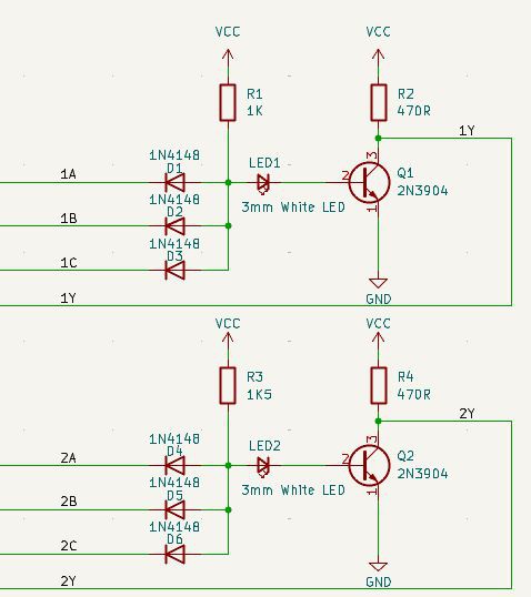
There are 3 input diodes, the low-cost and 4nS fast 1N4148.
These are arranged in common anode with the anodes pulled to VCC with a 1K resistor. This is the classic "wired AND", all three inputs need to be at logic 1, or floating, for the common anode node to be high.
The white LED presents a "voltage hurdle" of approximately 2.5V, which needs to be overcome before the transistor will saturate in the on condition.
So the diodes provide the AND function and the transistor inverts this to create NAND.
Additional inputs can be created just by adding more diodes .
I found a 1K input pull-up resistor to work well, but I experimented with 1K to 10K.
I did not get a good response at 10K. The lower gate has a 1K5 pull-up shown, but the boards I assembled settled with a 1K pull-up.
Similarly the collector load resistor, I found 470R to be good. I purchased resistors to try 620R, 750R and 1K.
I didn't manage to duplicate Mats Engstrom's 10K/1K version. (More investigation required).
The NPN transistor can be either a 2N3904 or BC547C. These have a complementary pin-out, CBE versus EBC. So the BC547s should be inserted "backwards" into the pcb. There are also 2 variants of the lead spacing, either 1.27mm or 2.54mm. The pcb accepts both variants.
Here is the bare pcb:

and populated:

The completed pcb uses a 26-way right-angled pin header. This gives connection to every input, every output, VCC and GND.
J3 (far right, unfitted) allows the flipflop to be used either in a counter circuit or a shift register circuit.
The pcb is 66.5 x 23.5mm.
Testing.
The flipflop was tested at clock frequencies up to 12.5MHz. Divide by two was successful up to 12.5MHz.
A 4-bit binary ripple counter was constructed from 4 pcbs. It ran successfully with a 6.25MHz clock.
More testing is required, to assess the range of workable VCC, the setup and hold times, and the propagation delay and fan-out of the basic 3-input gate.
I am pleased with the performance, so far of the White LED Logic gate. I believe that it can be used as a reliable building block for more complex designs, both combinational and sequential.
Six transistors per flipflop (6T)is a lot, DEC managed it with 2 transistors (2T). Now that I have a stable PCB, and not "sloppy" breadboards, I hope to see if I can get down to a 2T solution.
Yes - transistors are cheap, but with a 2T solution, you can cut your component cost by a factor of 3, and increase the logic density by a similar amount.
Discussions
Become a Hackaday.io Member
Create an account to leave a comment. Already have an account? Log In.