 Anders Helgesson
To know how the GSD really work we need to know all the unknowns of the hardware and capturing the communication between the GSD and the software can provide us with more information.
Instead of using wireshark directly to do the capture I decided to use dumpcap as it is. I wrote a script that is run as root that uses dumpcap on the usb interface the GSD uses, when the capture is over it will move the file over to my user, it renames and adjust the permissions. Then I'll analyze the dumps in wireshark.
Captured two dumps, one when reading a SLG46826V and a full programming cycle for my diavox SLG46826V.
Analyzing gets old pretty fast tabbing between the datasheets and wireshark to see what the bytes and bits does. So I decided to make a wireshark dissector for the MCP2221A.
After researching some more about it, I enlisted chatGPT to do the bulk of the work or so I thought... Cobbling together unfinished lua dissector script with chatGPT for help, got me some more information.
ACMP (mcp2221a GP3) is being used as ADC.
How do you get the ADC data from the MCP2221A?
According to the datasheet it's in the status command reply.
Byte 50, 51 = ADC channel 0
Byte 52, 53 = ADC channel 1
Byte 54, 55 = ADC channel 2
Pin out description it says ADC1, ADC2 and ADC3 while it also says "3 x (16-bit) little-endian ADC channel values (CH0 LSB, CH0 MSB, CH1 LSB, CH1 MSB, CH2 LSB, CH2 MSB)."
Here is the first status reply I found in one of the dumps.
Status reply
10 00 00 20 78 00 00 00 00 02 00 02 00 02 78 00
10 00 10 28 00 60 01 01 00 00 f1 79 f0 00 00 00
30 00 1b 00 02 27 13 45 03 00 00 26 90 1c 41 36
31 32 00 00 00 00 08 00 01 03 48 02 00 00 00 00
Since bytes 50-55 is the ADC channels we get this.
ADC1: 0x0000
ADC2: 0x0000
ADC3: 0x0008
I noticed this that both the Get SRAM reply and Status reply seems to contain the ADC values. Get SRAM command reply have most bytes including the last 32 bytes marked as "Don't care" in the datasheet. Going to have to deal with more don't care and any values later.
Get SRAM reply
61 00 12 04 78 12 88 1c cf 2d 06 d0 80 32 00 00
00 00 00 00 00 00 10 08 00 0a e1 75 f0 00 00 00
30 00 1b 00 02 27 13 27 00 00 00 26 90 1c 41 36
31 32 00 00 00 00 0a 00 00 03 65 02 00 00 00 00
ADC1: 0x0000
ADC2: 0x0000
ADC3: 0x000A
The values are little endian. So the data for ADC3 from status reply above here its has the value 0x0008 which is 8 in decimal. 0x000A is 9 in decimal so the values are close enough. More testing is required. Anyway let's continue.
To calculate the actual voltage we have to know a few things. How many bits the ADC can do, in this case it's 10-bits, the voltage divider k value and the voltage reference.
The maximum value a 10-bit ADC can get is 1023.
The voltage divider has k of 4.666.
The formula to get the voltage is
voltage = adc_value / max_adc_value * vref * k
I know from the captured data that the ADC3 is setup with 4.096 V as reference.
First status reply message.
( 8 / 1023) * 4.096 * 4.666 = 0.149 Volts
Status reply in the middle of the dump
(138 / 1023) * 4.096 * 4.666 = 2.57 Volts
For the last status replay message in the dump.
(74 / 1023) * 4.096 * 4.666 = 1.38 Volts
Not sure what is going on or if my calculations are correct. I'm sure I set the voltage to 3.3 volts in the greenpak software. Perhaps there is some calibration? I'll figure it out later with some more testing.
The maximum voltage the ADC in this case see handle is
(1023 / 1023) * 4.096 * 4.666 = 19.11 Volts.
Now why is the voltage divider set like this wasting precision?
There is no input protection before the voltage divider, so to protect the inputs of the MCP2221A and PowerPAK from overvoltage the voltage divider is set up like this.
The maximum voltage the PTC can handle is 16 volts.
So if you by accident feed 12Volts into the GSD VDD_OUT it will probably not release magic smoke. The zener will sink the current, the PTC trip and the device will most likely it will still work after the PTC cools down.
12 Volts on the SDA or SCL pins would release the magic smoke from the level shifter. It's not possible cost wise to protect devices from all the mistakes the users could make.
Let's now look at the first Get SRAM reply using my dissector in wireshark.
GP0 : SEL0
GP0 Settings: 0x10
    ...1 .... = GP0 GPIO Output Logic Value: True
    .... 0... = GP0 GPIO Direction: Output
    .... .000 = GP0 Designation: GPIO operation (GPIO0) (0x0)
This is SEL0 which enabled at the start. It's thus written into the flash of the MCP2221A as a default value. This is most likely the PowerPAK. Have investigate further to know for sure.
GP1 : ERROR
GP1 Settings: 0x08
    ...0 .... = GP1 GPIO Output Logic Value: False
    .... 1... = GP1 GPIO Direction: Input
    .... .000 = GP1 Designation: GPIO operation (GPIO1) (0x0)
This the ERROR pin and it is set up as an input pin so when an error occur in the PowerPAK logic this pin will be high. This would tell the software an error has happened.
GP2 : SEL1
GP2 Settings: 0x00
    ...0 .... = GP2 GPIO Output Logic Value: False
    .... 0... = GP2 GPIO Direction: Output
    .... .000 = GP2 Designation: GPIO operation (GPIO2) (0x0)
This is SEL1 and it is setup as an output which default value is False. Most likely SEL1 is the target greenpak.
GP3 : ACMP
GP3 Settings: 0x0A
    ...0 .... = GP3 GPIO Output Logic Value: False
    .... 1... = GP3 GPIO Direction: Input
    .... .010 = GP3 Designation: Alternate function 0 (ADC3) (0x2)
Here we can see that GP3 is setup as ADC3.
To truly confirm that SEL0 is PowerPAK and SEL1 is the target GreenPAK. I have to check the I2C traffic.
The first I2C write performed does a write to `0xF4` with the data `0b00000001`.
Now the datasheet for the SLG46582 doesn't have the address bytes in it like the SLG46826. First convert the 0xF4 to decimal, then multiply by 8. Which is 244 * 8 = 1952.
In the datasheet for the SLG46582 register 1952 is the least significant bit of the byte containing all the I2C virtual inputs. `0xF4` is the byte that contains all these I2C accessible registers which can be used in the logic inside the PowerPAK.
The data written to this address is `0b00000001` and since no mask is set this sets registerbit 1952 to 1 and the rest to 0. This could mean either that only the 1952 registerbit is used or that they are just initialized like this.
In the SLG46826 byte 0xF4 is reserved and not used.
This confirms that SEL0 is the PowerPAK, which means that SEL1 is the target.
The last unknown is how the logic is wired inside the PowerPAK. To get this I can just use my generic mcp2221a driver change the PID and VID in it to target the GSD and do the dump command in my CLI software. Don't need add GPIO support in my software even as it starts with SEL0 set true.
I managed to dump the SLG46582 it was not read locked and feeding it into the greenpak designer software give us this.
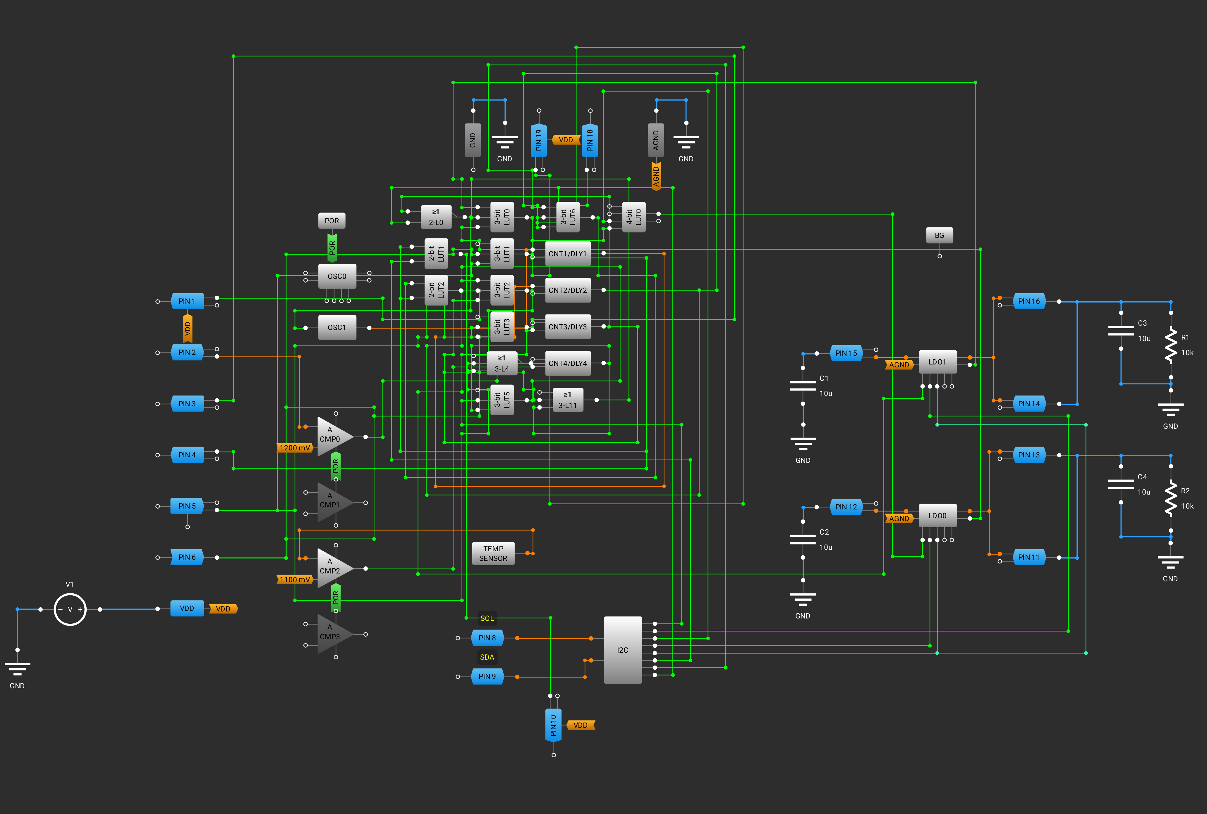
We now have all the data required to exactly know how the GSD works in hardware, but that looks like a mess.
Next time I'll reorder the logic and add labels, so it's easier to see what goes on inside the SLG46582.
Discussions
Become a Hackaday.io Member
Create an account to leave a comment. Already have an account? Log In.