Normally we operate BJTs with the collector high, and base voltage variable (and current-limited), relative to the emitter (for expedience, I'll use NPN polarity here; for PNP, everything is flipped, plus for minus!). This gets us the common set of circuits, for power/logic switching, current source/mirror, amplifier, clamper, and so on, and even analog switching with some effort (if somewhat approximate).
Inverted Mode
What happens if collector voltage goes below emitter? Recall that an N-P-N transistor reads the same backwards (the difference lies in the details); indeed, it still works, albeit not usually as well. This is inverted mode. Besides having lower "VCE", hFE is usually quite small -- a typical 2N3904 might hit 5 or 10. Both are a consequence of the doping levels being backwards; the emitter "emits" better when it's highly doped, and high doping level causes a narrow depletion region, hence the low breakdown voltage (typ. 6-8V).
Transistors have been designed for inverted mode operation. 2SC2878 (obsolete/vintage) and 2SD2114K (a rather tasty little transistor in its own right) come to mind. Typically, VEB is higher, and some effort has been made to keep reversed hFE comparable (typically still lower than forward, but manageably so). They aren't usually specified in terms of inverted characteristics, but a resistance spec is added, which one can assume is an acceptable ohmic approximation (i.e. it has low distortion while saturated).
Another consequence of inverted operation: the built-in potential due to the doping gradient (heavier in emitter, lighter in collector), while it doesn't manifest as free energy (of course), it does affect Vce(sat). 2N3904 might (forward) saturate at some 10s of mV, a respectable level, but doesn't go any lower, even at very small IC, or large IB (indeed, IB eventually works against you due to emitter resistance). Inverted or "VEC(sat)" can be single mV. In past centuries, engineers used this to make high accuracy D-A converters, before integrated versions (or MOSFETs) were developed. (JFETs were a competitive option, which might be chosen for or against based on other factors like switching speed or charge injection.)
Emitter Breakdown
Normally, this is an undesirable characteristic, limiting the input voltage of a differential amplifier for example, or causing aberrant behavior in switching circuits (breakdown, in a blocking oscillator, also called a RCC (ringing choke converter), a type of single-transistor self-oscillating converter, typically causes runaway operation, as it returns charge to the base circuit, obviating the control loop!). It might be used intentionally as a cheap and noisy zener diode. But quirks lurk in the shadows:
Avalanche breakdown in silicon is accompanied by visible light emission. Not much, seeing as silicon is so opaque to visible light, but enough that some is visible at the edge of the junction (i.e., where it reaches the surface, giving off a faint greenish to orange glow). When silicon absorbs light, free charge carriers are produced -- a transistor is a photodiode or solar cell with extra steps, and low gain -- and thus a photocurrent is produced, in addition to the free charges already swarming about due to avalanche breakdown. It's not actually important that photocarriers are generated -- the penetration depth of visible light in silicon is some µm -- but more that, regardless of source (avalanche or photolytic), the free carriers diffuse into nearby junctions, carried across by the built-in potential, and thus a voltage can develop -- independent of other terminal voltages.
This famously led to a Bob Pease article, posing the riddle:
(Bob Pease, What's All This R-C Filter Stuff, Anyhow?, Pease Porridge, Electronic Design, March 18, 1996. Archived scan (p.13): http://www.introni.it/pdf/Bob%20Pease%20Lab%20Notes%20Part%203.pdf)
Using a high-impedance meter, approx. -0.4V is generated. The current is quite feeble, but one might find application in pulling an op-amp's output to true zero, in a single-supply setting (where a pull-down is otherwise unavailable, and only some mV/µA is necessary).
Astute Hackaday readers will recall a familiar article: https://hackaday.com/2021/06/10/an-explanation-of-a-classic-semiconductor-riddle/
It's also been referenced on Stack: https://electronics.stackexchange.com/a/701789/311631
Collector Breakdown
Actually, this applies to emitter breakdown as well (an oscillator, at modest supply voltage, can be created that way), but its most impressive feat is found from the collector side.
Collector breakdown is not a single value, but depends on what's happening at the base:
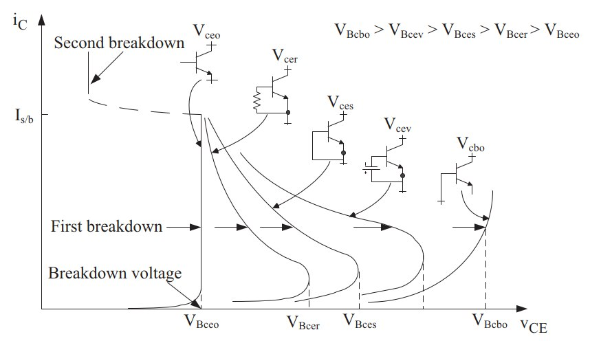
C-B breakdown is as good as a regular zener (avalanche) diode, albeit limited by base current rating. The others, are weird: there is a region of negative resistance, until further breakdown or destruction. The various curves form a continuum, depending on how strongly (and by what V(I) curve) leakage current is removed from the base. (Note that, for VCEO, C-B leakage is effectively multiplied by hFE, so we expect IC (at lower VCE) to be highest in this mode as well.)
The negative resistance region is not straightforward to use: in fact, it's rather slippery and abrupt. Second breakdown, as usually documented, is a slow (thermal) process (i.e., takes ∼ms to develop), but a rapid breakdown mechanism also exists.
The mechanism works something like this: at high electric field strength in the C-B junction, loose charges (thermal leakage) collide with ions, freeing more charge carriers -- impact ionization -- which free more and so on in cascade. As breakdown voltage is approached, the multiplication factor increases, and so too the scale of the avalanche discharge (or Townsend discharge). This is a highly local phenomena: perhaps 100nm wide, and the high power density raises the temperature significantly (supposedly, ∼300°C) -- or, more or less equivalently, the concentration of carriers can be so large as to turn the local area intrinsic and highly conductive. (I suppose this needn't be equivalent if it's not in thermal equilibrium with lattice phonons at this time scale; which, I don't know about offhand. Hence, "more or less" equivalent. In any case, there's no functional difference for us here.) The high temperature (or carrier concentration) further punches through the base layer, effectively shorting C to E with low resistance -- 2N3904 typically gives about 10Ω in this state. The energy stored in CCB is (nearly) instantaneously discharged, which contributes to the rapid and intense local heating. The small scale of this phenomenon is evident in its recovery speed: if it's thermally mediated, a recovery time of 10-20µs is quite rapid indeed. Alternately, it's typical of the recovery time of carriers in (intrinsic) silicon; if not of carriers in a typical BJT in-circuit (which range from 10s ns for conventional types with strong base drive, to maybe 20µs for a turn-off condition of merely IB = 0).
I learned about this effect many years ago, and put together this little cluster of components to demonstrate it. A PH2369A is the active device, breaking down at about 80V:

Basically a 7pF capacitor gets discharged into the output transmission line; a 10k resistor biases the transistor in the "VBcer" mode, 100k supplies high voltage, and a 47Ω is in series between emitter and output. Supplied by 80-100V, it free-runs with an unstable repeat rate (say 90-100kHz) and a sharp output spike:

Measured with my trusty (at the time) old (at the time; even older now..!) Tek 475, the rise time and pulse width challenge the 200MHz bandwidth of the venerable instrument already. This is at the fastest sweep rate, 10ns/div.
More avalanche explanation and design ideas can be found in this paper: High voltage pulse generation using current mode second breakdown in a bipolar junction transistor, R. J. Baker, Review of Scientific Instruments, 62 (4), The American Institute of Physics: 1031–1036 (1991); downloaded from: https://cmosedu.com/jbaker/papers/1991/RSI621991.pdf The Wikipedia page is also quite informative, actually: https://en.wikipedia.org/wiki/Avalanche_transistor Diodes Inc. (née Zetex) also has an excellent appnote on them: https://www.diodes.com/assets/Part-Support-Files/FMMT413/201342.pdf
The intensity of this effect can be hard to appreciate; most transistor switching (again, with general-purpose types) tops out in the 10s of ns range, so something special is definitely going on. Note that 100V discharging into 50Ω is 2A peak, which these small transistors can easily handle -- despite the current filament being so minuscule. The current densities really are tremendous here. It should be no surprise, it is easy to exceed as well: shockingly, fairly small transistors like FMMT413 can handle pulses in the 20-40A range, with some limits on pulse duration and lifetime. Large power transistors are simply too much, though: a typical horizontal output transistor for example (say, 10A 1500V VCBO) is destroyed in the process. The mechanism of failure itself is interesting; the device isn't blown up (there's not nearly enough energy for that), but it's probably locally fused, if not vaporized. The failure mode is a shunt resistance C-E, perhaps some 10kΩ. Implying it perhaps melted through, mixing dopants and shorting through at a point -- but the short is small and thin compared to the large junction (whose capacitance powered the destructive event) so the resistance is surprisingly high as "shorts" go. So, transistors up to one or a couple amperes rating are about the most practical in this application, which the above references seem to agree on.
Bonus: Abusing a Vacuum Tube
In a somewhat more recent experiment (ca. Feb 2021), I employed the above effect to probe a more archaic device's limits:
A summary exists here: https://www.eevblog.com/forum/projects/how-fast-are-tubes-for-switching/msg4676896/#msg4676896
There are two interesting types of commercial receiving tubes for fast pulsing operation: pulse-regulator types like 6HV5, and horizontal sweep output types like 6KD6, 6LB6, EL519, etc.
The pulse-reg types are fascinating, in a frustrating sort of way. They're clearly leftovers from the sweep production line: basically the screen grid is removed, so they have SFA perveanace; and probably the grid is wound finer, giving quite high gain (mu and gm), ...if only you can bias it into conduction at any reasonable voltage. Their intended purpose is to sap power from the flyback pulse in a color TV set, regulating picture width and 2nd anode voltage; hence they only need to conduct at high voltages anyway, and the peak current isn't too important (but is potentially on par with the sweep's peak current, so it's no accident the cathode is as big!). I've seen them suggested for (but never with published results!...but why?! :) ) direct-drive ESL application, high voltage regulation, RF amplification, etc. Well, as a linear shunt reg I guess it would be okay, but as a pass device, laughable. Any amplifier needs a ridiculously high load impedance, and reasonable plate voltages (say, 1 or 2 kV) require class 2 (grid current flows) operation, perhaps even statically just for a meager class-B bias(!). So, they look impressive, but they really just don't have anything to offer, in basically any circuit but what they're intended for, and even that one seems a bit of an afterthought, a hack job.
As it turns out, even in relatively deep forward-grid drive, they really just don't turn on very hard. In a circuit as so:

I measured:

This was 6HV5, driven to +60Vpk grid (Ch3, 10x), drawing about 2A peak plate current (Ch1, 100x).
Satisfied that these types will never be interesting, I moved on to sweep tubes; I tested a fairly late-generation type, 6LB6:

It did better (this time, into 500Ω load, with a double-peaked PFN driving the grid to about +20V), but still not all that impressive in the grand scheme of things -- the most disappointing part here is the whole time spent slewing the (seemingly fairly modest) plate capacitance of 18pF, which implies a displacement current of 1.35A so is very much representative of the system. Alternately, 18pF * 500Ω = 9ns time constant, so we shouldn't expect to do much better than this anyway.
So, that's driving a sweep tube to a peak output power around 3.2kW -- not bad, considering, but still easily surpassed with modern MOSFETs, even Si ones (if just barely; handily so by SiC and GaN).