yjmwxwx
Description
LCR Digital Bridge Capable of Measuring Battery Internal Resistance Based on Renesas R7FA2E1A7 MCU
1. Project Function Introduction
As an amateur electronics enthusiast, I usually need to measure battery internal resistance and the impedance of electronic components. Switching between two instruments is quite cumbersome. Many open-source bridges omit the DC-blocking capacitor and protection circuit, making it impossible to directly measure battery internal resistance. Connecting an external DC-blocking capacitor is not very convenient either. Therefore, I designed an LCR digital bridge that can measure battery internal resistance by myself, while verifying my own ideas. The design adopts dual-channel acquisition and multi-ADC port sampling to improve reading resolution.
Since I am an amateur enthusiast, this project was challenging for me. As a result, the final product is not very user-friendly and only reaches a "barely usable" level.
- Measurement Frequencies: 1kHz, 10kHz, 100Hz
- Impedance Measurement Range: 1mΩ to 10MΩ Measurable parameters include: battery internal resistance, series capacitance, series inductance, series resistance, series reactance, D-value, Q-value, phase angle, and impedance magnitude.
Due to the multiple frequency options and wide measurement range, some gears may have bugs. There are also issues with the auto-ranging function, which sometimes fails to switch to the correct gear.
2. Project Attributes
This project is publicly released for the first time. Part of the circuit is referenced from open-source bridges, while the program is original.
3. Open-Source License
GPL 3.0 open-source license, with both hardware and software being open-source.
4. Hardware Part
The power supply part uses 18650 batteries for power supply, with DW01 protection and 4056 charging functions. SW1 serves as the main power switch of the entire device. U4 converts the voltage to 3.3V. The maximum power consumption does not exceed 40mA when the clips are short-circuited.
Key Notes on Terminology
- MCU (Microcontroller Unit): The core control chip of the device, here referring to the Renesas R7FA2E1A7.
- DC-blocking capacitor: A capacitor used to isolate DC signals while allowing AC signals to pass, a critical component for measuring battery internal resistance.
- 18650: A common cylindrical lithium-ion battery specification (18mm diameter, 65mm length), widely used in portable electronic devices.
- DW01: A typical lithium battery protection IC, used to prevent overcharging, over-discharging, and short-circuiting of the battery.
- 4056: Refers to chips like TP4056, a common lithium battery charging management IC, supporting constant-current and constant-voltage charging.
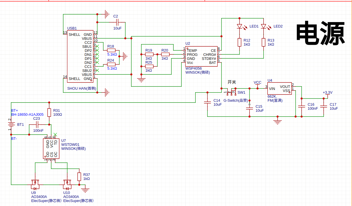
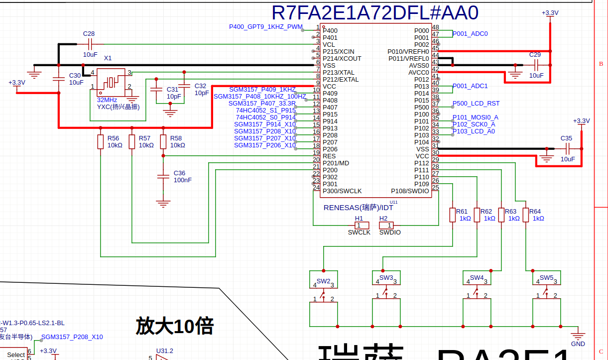
The Renesas R7FA2E1A7 MCU is used as the main controller, with a 32MHz crystal oscillator. Although the maximum frequency specified in the datasheet is 20MHz, an overclocking operation was performed to verify the idea of using 4 ADC ports for sampling. The sampling rate is 50KHz, and all collected data need to undergo DFT operations, resulting in a relatively large computational load. The DFT calculation frequency is around 70K, which just allows interrupts to be generated, hence the overclocking.
Pin functions:
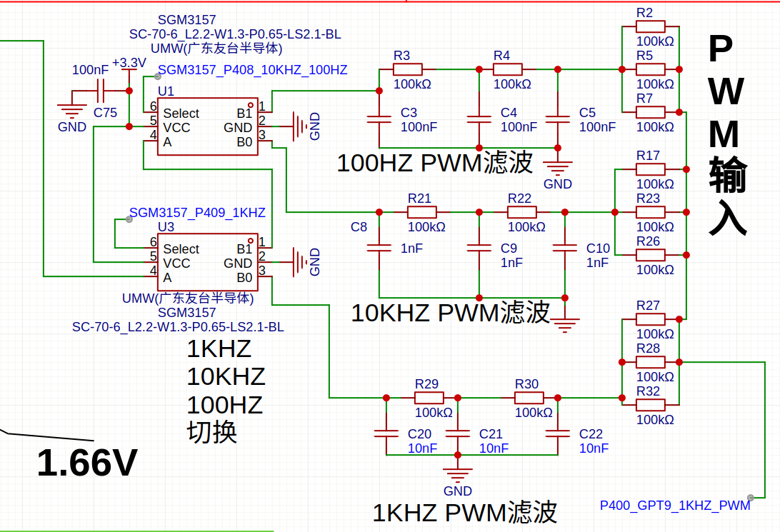
- P400 outputs PWM. P409 and P408 switch the PWM filter circuit through an analog switch to serve as the excitation source.
- P407 is the 33.3Ω gear switch analog switch. Since the on-resistance of the 74HC4052 analog switch is relatively large, which cannot meet the requirements of the lowest gear, a 3157 analog switch is connected in parallel in the 33.3Ω gear to reduce the on-resistance.
- P915 and P914 are the control ports for the 74HC4052 gear switch, used to switch resistors of different gears.
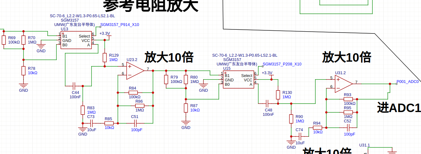
- P206 and P207 are the gain switches for the measured components, each providing a 10x gain.
- P208 and P914 are the gain switches for the sampling resistors in the internal V/I circuit, each also providing a 10x gain.
- P300 and P108 are SWD ports. The JLINK V9 needs to be connected with 4 wires: 3.3V, GND, SWDIO, and SWCLK.
- P000 and P001 are the resistance sampling ports of the V/I circuit. P013 and P014 are the sampling ports for the measured components, using dual-port acquisition to verify the idea of improving resolution.
- The ADC directly uses AVCC and AVSS as references and is directly connected to the digital power supply of the MCU, which may increase ADC reading fluctuations.
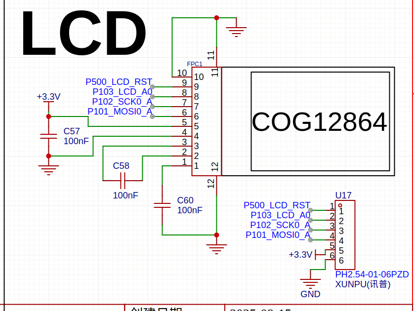
- P500, P101, P102, and P103 are LCD driving ports.
- P109, P110, P111, and P112 are four buttons.
The PWM filter circuit directly adopts RC filtering, which converts the PWM signal into a sine wave after RC processing—this design simplifies the MCU programming complexity. Two 3157 analog switches are used to switch between three sets of RC filters, which serve as the excitation source.
However, the RC filter circuit has a relatively large component attenuation. This significant attenuation leads to a weak output signal, making it more susceptible to interference. Additionally, the weak signal requires high-gain amplification in the subsequent stage, which results in relatively large temperature drift. That said, due to the adoption of dual-channel acquisition in the system, the temperature drift actually has little impact on the final measurement reading.
### Key Terminology Supplement
- **RC filtering**: A passive filtering circuit composed of resistors (R) and capacitors (C), which filters out unwanted frequency components in the signal. Here, it is used to convert the square-wave PWM signal into a smooth sine wave.
- **Temperature drift**: A phenomenon where the performance parameters of electronic components (such as the gain of amplifiers) change with temperature variations, which may affect measurement accuracy if not mitigated.
- **Excitation source**: The signal source that provides a stable input signal to the measured component, which is essential for impedance measurement in LCR bridges.
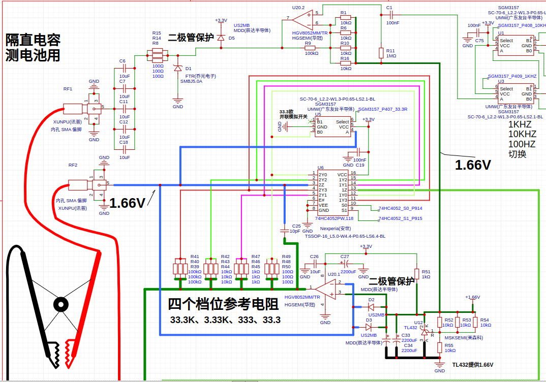
After RC filtering, the signal is passed through capacitor C1 for DC blocking and then shifted up by 1.66V before entering pin 2 of operational amplifier U20 for high-gain amplification. A lower amplification factor here would cause high-frequency oscillation. The output of the op-amp is fed to RF1 via a 33.3Ω resistor and a 50μF capacitor, with D1 and D5 providing protection.
RF1 and RF2 are connected to Kelvin clips to conduct current. The inverting amplification of U20 (pin 1) uses a 74HC4052 to switch between four gain levels corresponding to resistances: 33.3Ω, 333Ω, 3.33kΩ, and 33.3kΩ. For the lowest resistance level, since the 74HC4052 has a high on-resistance, a 3157 analog switch is connected in parallel to reduce the resistance.
A TL432 provides a 1.66V reference ground voltage, and together with D2, D3, C33, and C34, forms an input protection circuit. The four range resistors also adopt a four-wire measurement method. Conveniently, the 74HC4052 has two sets of switches to support this configuration. This part of the circuit references open-source bridge designs.
### Key Terminology Notes
- **DC blocking (C1)**: A capacitor used to isolate DC components in the signal, allowing only AC signals to pass through.
- **Voltage shifting (1.66V)**: Adjusting the signal's DC level to match the input range of the op-amp, ensuring proper amplification.
- **Kelvin clips**: A precision connection method that separates current-carrying and voltage-sensing paths, minimizing contact resistance errors in low-resistance measurements.
- **Four-wire measurement**: A technique using two wires to carry current and two additional wires to measure voltage across the DUT (Device Under Test), eliminating lead resistance interference.
- **TL432**: A shunt voltage reference IC, providing a stable 1.66V reference here for consistent signal biasing and protection circuit operation.
The following is a dual-channel amplification circuit, which separately amplifies the voltages across the measured resistor and the range-switching resistor. Each channel is set with two amplification factors, forming two amplification gears: 10x and 100x.
However, the impact of temperature drift on the readings of the dual-channel amplification is relatively obvious. When measuring the same resistor at different times, the deviation is quite large, which is less stable than switching back and forth with a single channel.
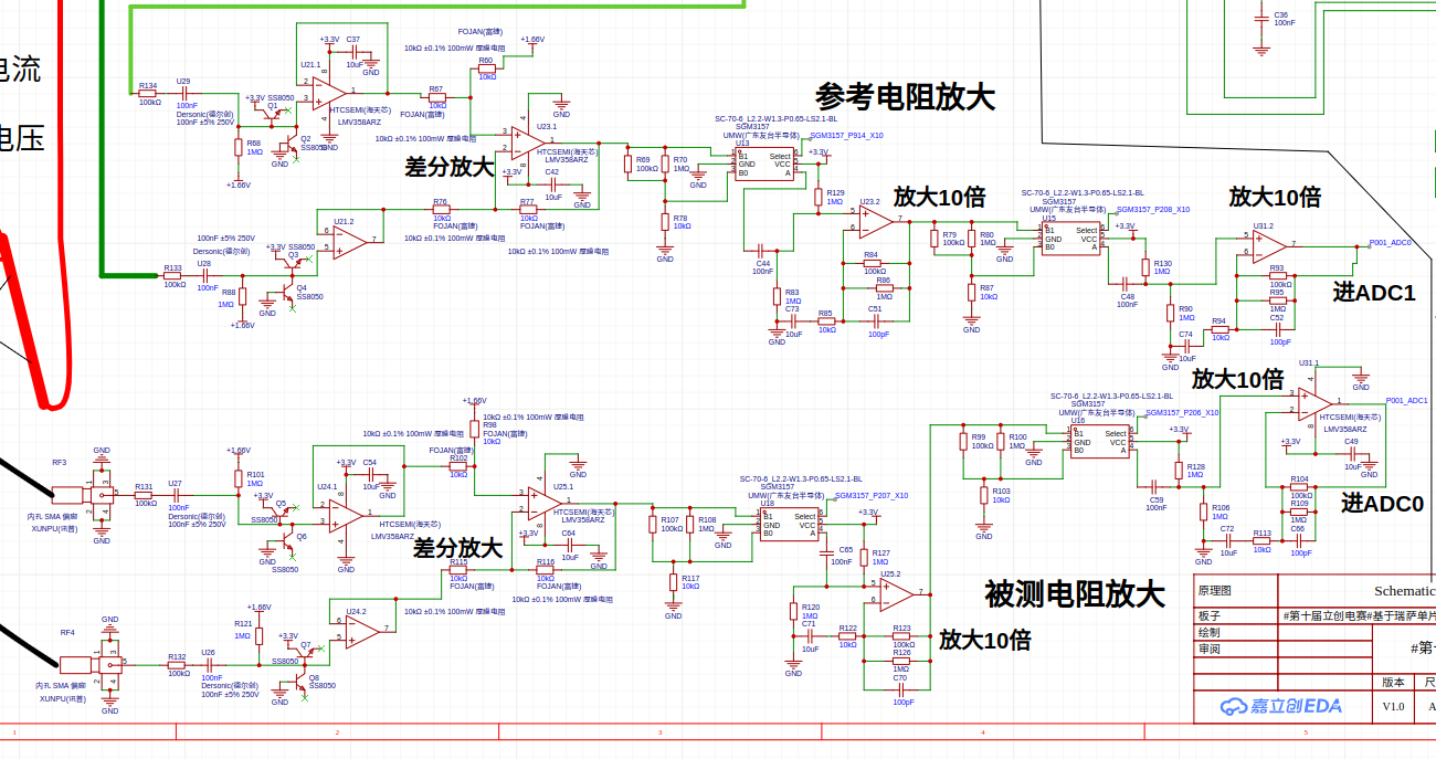
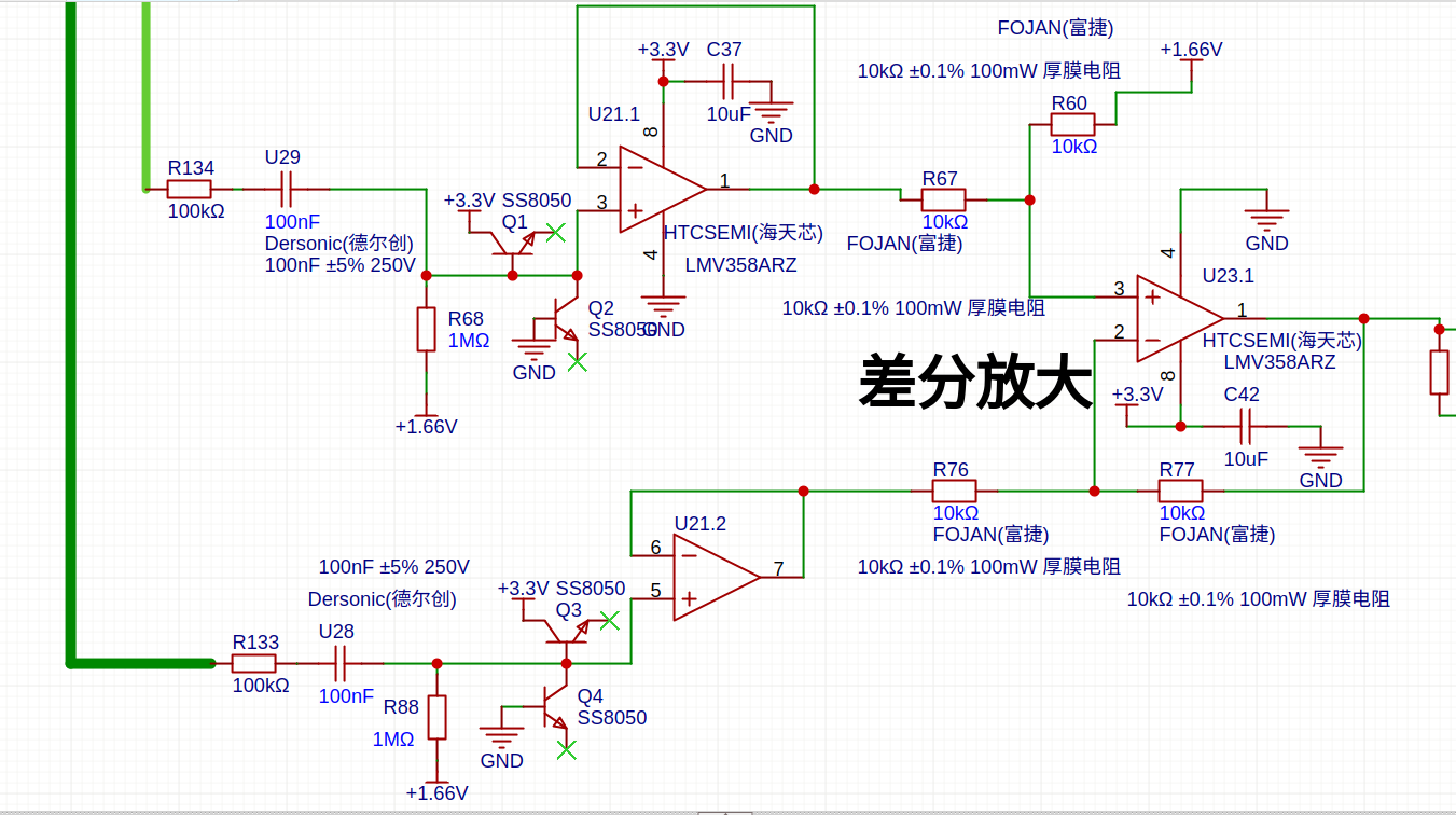
The voltage across the reference resistor or the measured resistor is first passed through a 100KΩ resistor and a 100nF capacitor for DC blocking. It is then shifted up by 1.66V via a 1MΩ resistor. An SS8050 transistor is used instead of a diode for protection to prevent damage to the operational amplifier. The processed signal enters the operational amplifier for follower output, followed by differential amplification through U23.1.
The LCD display still uses the previously purchased COG12865, with the ST7567 as the main controller. These were second-hand units bought for around 1 RMB each at the time, and they are no longer available now. To facilitate replication by other enthusiasts, pin headers for the LCD driver interface have been reserved, making it easy to design an adapter board.
When soldering the circuit, first solder the power supply section. Check that the 3.3V and 1.66V voltages are normal, then solder the analog circuit signal section. After soldering, check for short circuits before soldering the MCU. Note that the 3157 analog switch is prone to cold solder joints when soldered with a soldering iron. After completing the soldering, switch to the 30Ω range, clamp a 33.3Ω resistor, and observe that the V (voltage) and I (current) displayed on the screen are approximately equal, which indicates that the circuit amplification section is working properly.
## 5. Software Part
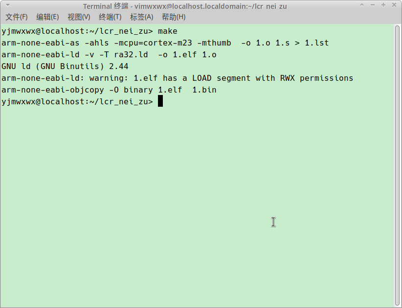
The source code and firmware are in their respective folders: 1.S is the source code, and 1.bin is the pre-compiled firmware.
To save the software project locally, use: `git clone git@gitee.com:yjmwxwx1/R7FA2E1A7.git`
Bug reports are welcome. Any provided bugs will be addressed and fixed with updates.
The compiler can be downloaded from the official ARM website: https://developer.arm.com/downloads/-/arm-gnu-toolchain-downloads
Alternatively, you can download GNU binutils and compile it yourself.
Simply enter `make` to compile the firmware.
For the software solution, 4 ADC ports are used for sampling to verify my own idea. Without comparison, it’s hard to tell the actual effect, but it should provide higher resolution.
This time, instead of using DTC (Data Transfer Controller) to transmit sampling data, ADC direct interrupts are employed for sampling and data processing, with a sampling rate of 50KHz (consistent across all three measurement frequencies). The 100Hz range is too slow; initially, only the 1KHz range was calibrated, while the 100Hz parameters were not fine-tuned, making it less functional.
Upon entering the ADC interrupt, DFT (Discrete Fourier Transform) calculations are performed to obtain the real and imaginary parts of both the measured resistor and the reference resistor. The impedance is then calculated using these four parameters through the following method:
### Impedance Calculation Method A detailed introduction to the CORDIC algorithm can be downloaded in the attachment.
1. The upper arm (real and imaginary parts) and lower arm (real and imaginary parts) are each rotated to 0 degrees using the CORDIC algorithm, with the rotation angles recorded simultaneously. 2. Subtract the lower arm angle from the upper arm angle; the angle difference represents the impedance phase angle of the measured component. Adjustments are needed if the difference exceeds 180 degrees. 3. Since the signal is rotated to 0 degrees, the magnitude of the impedance is directly calculated by multiplying the real part of the upper arm by the resistance value of the lower arm’s reference resistor, then dividing by the real part of the lower arm. 4. Calculate the cosine and sine values corresponding to the angle difference. 5. Multiply the impedance magnitude by the calculated cosine and sine values to obtain the series resistance and reactance.
### Capacitance and Inductance Calculation Method An online version of the program is available for mutual conversion between different parameters, which is suitable for verifying the performance of the self-made LCR meter. Refer to the attachment for the file.
### Calibration Algorithm Calibration requires individual adjustment of open-circuit, short-circuit, amplitude, and angle parameters for each frequency and range. To simplify programming, a manual calibration method is used, which is relatively cumbersome and requires patience:
- **Entering Calibration Mode**: Press both the range increment and range decrement buttons simultaneously. - **Navigating Calibration Menu**: Use the range increment/decrement buttons to switch between calibration items. - **Entering Parameter Calibration**: Press both buttons again to access the selected calibration parameter. - **Open-Circuit Zeroing**: Adjust until the value after "I=" on the LCD fluctuates around 1. - **Short-Circuit Zeroing**: Adjust until the value after "V=" on the LCD fluctuates around 1. - **Amplitude Calibration**: First set the main parameter menu to display the absolute value of \( Z \), then enter amplitude calibration. Clamp a known resistor within the current range and adjust until the reading matches the resistor’s value. - **Angle Calibration**: Set the main parameter to capacitance or resistance, and the secondary parameter to angle display. Enter angle calibration, clamp a known capacitor or resistor with a predictable angle for the current range, and adjust until the angle reading matches.
- **Saving to FLASH**: Hold the secondary parameter switch button, then press the main parameter switch button. The screen will display "Calibration Completed" to confirm saving, ensuring calibration parameters persist after power-off.
For accurate measurement of milliohm-level components, amplitude calibration alone is insufficient; short-circuit calibration must also be performed. After completing the above steps, clamp a 1mΩ resistor and use short-circuit calibration to adjust the display to 1mΩ.
### Range Mode Switching The auto-ranging function for the current range is not fully reliable. To switch to manual mode, hold the range increment button. The letter "A" on the screen (indicating auto mode) will disappear; its presence indicates auto mode is active.
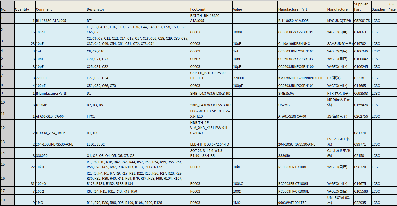
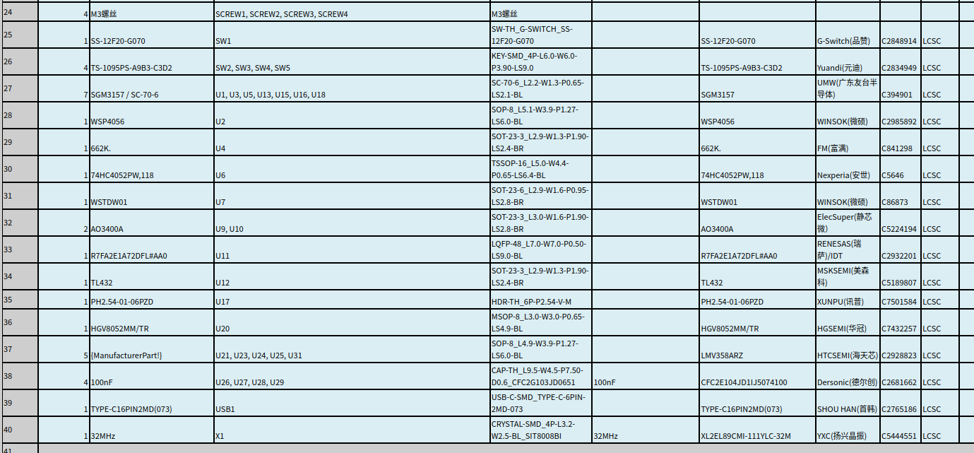
## 6. BOM List