 Hiroyuki OYAMA
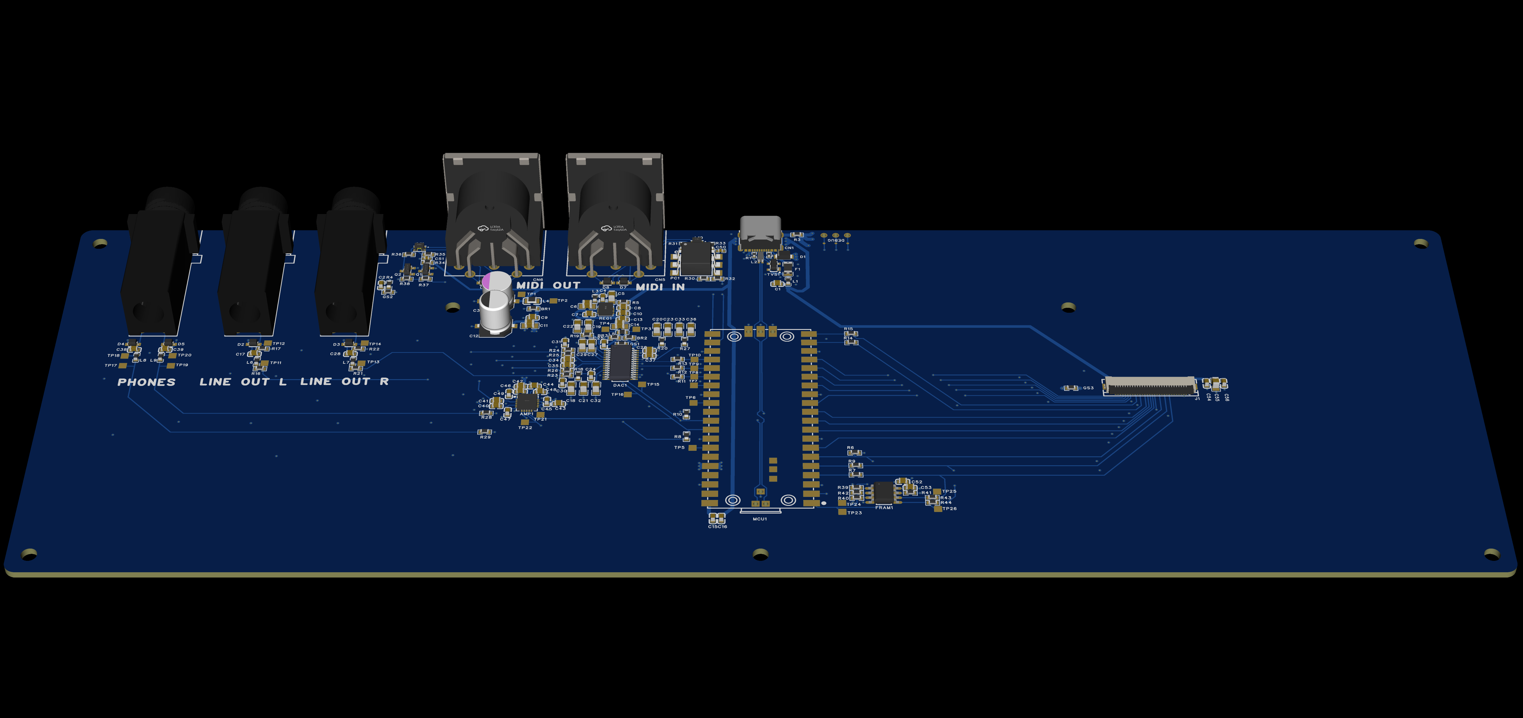
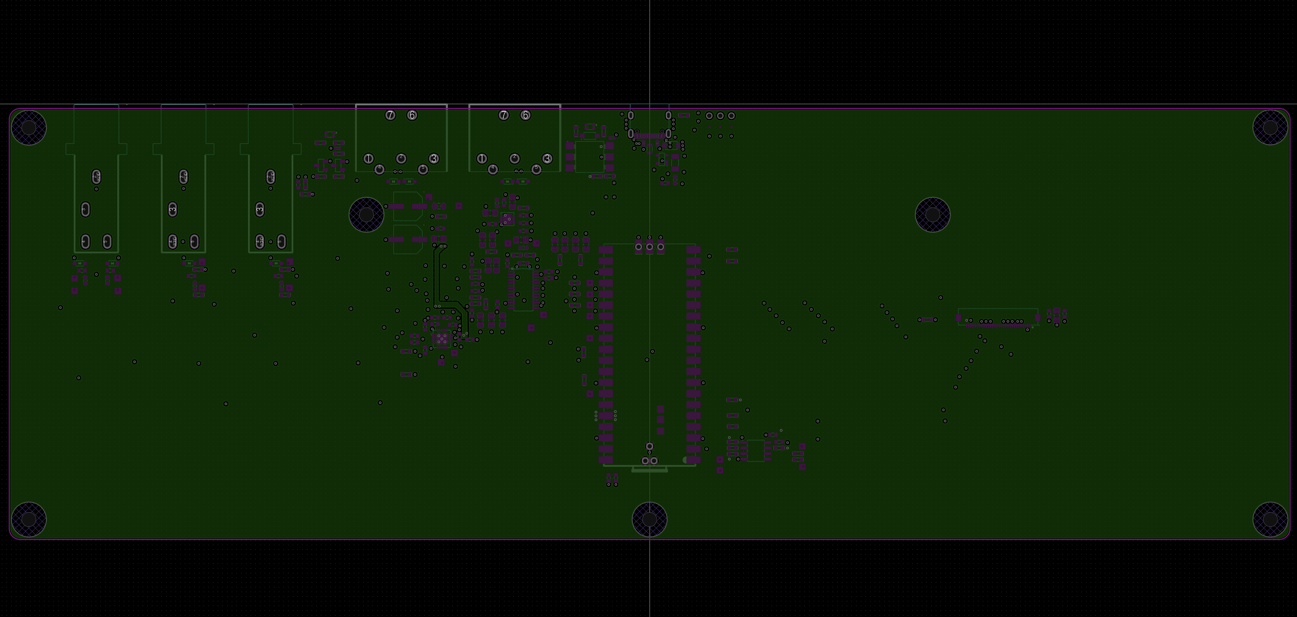
The main board of Darśana is almost complete.
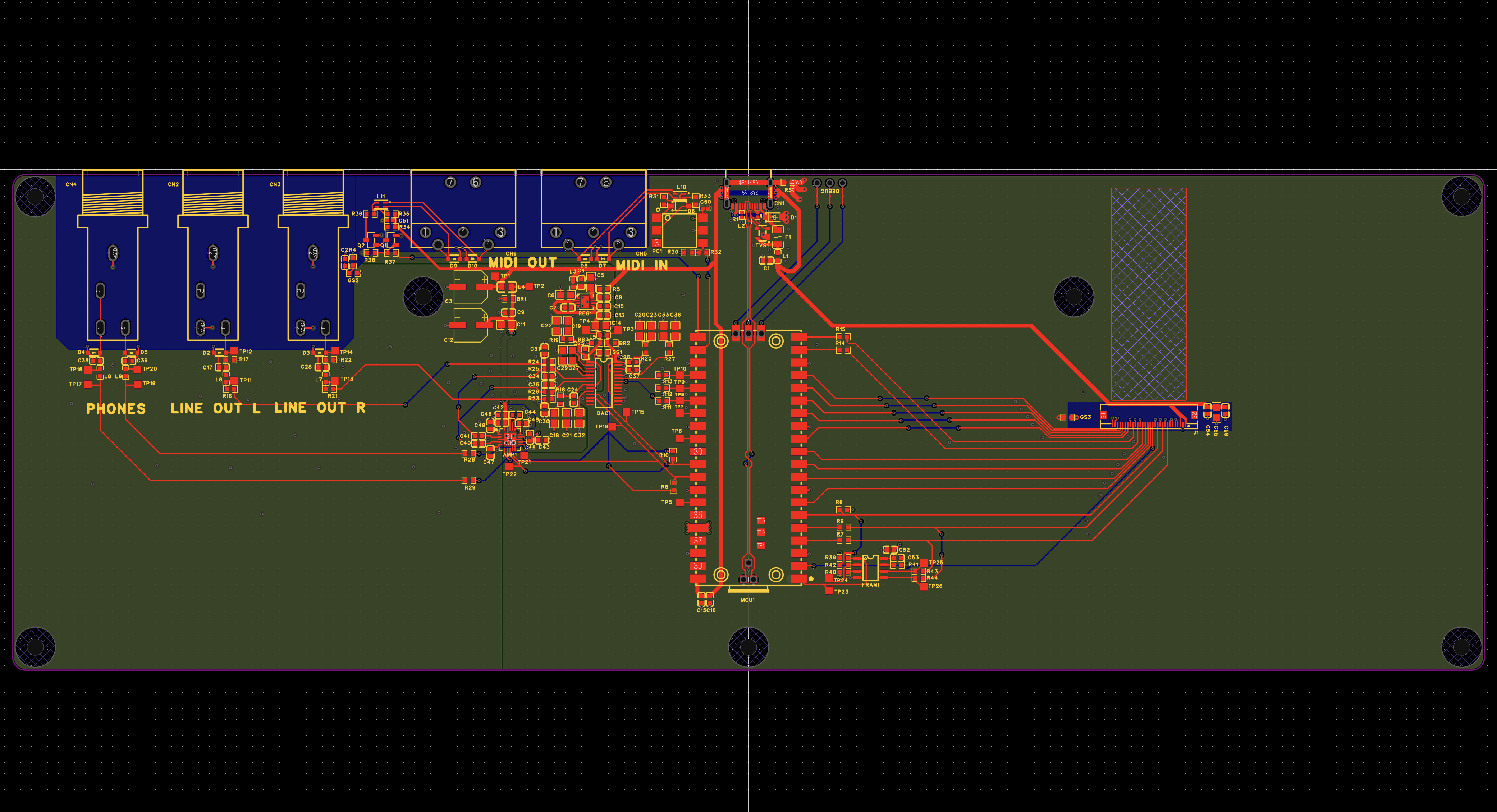
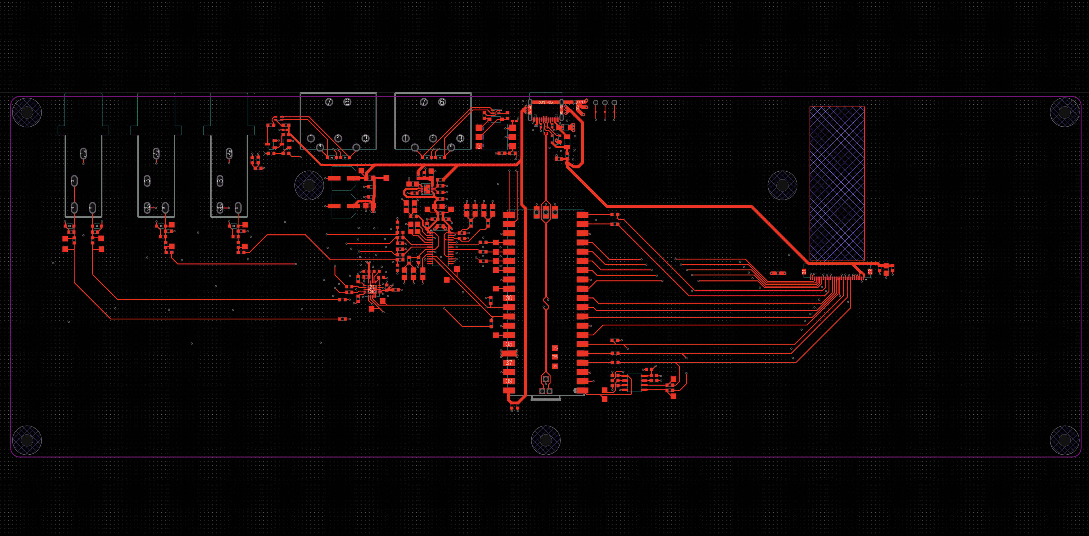
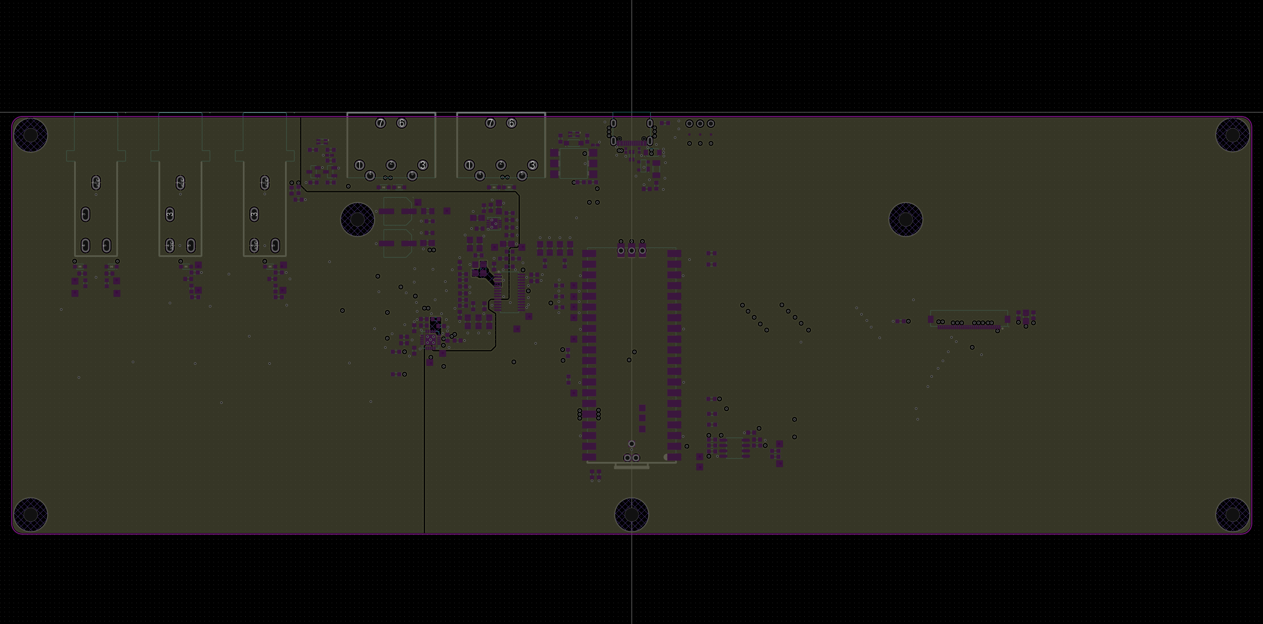
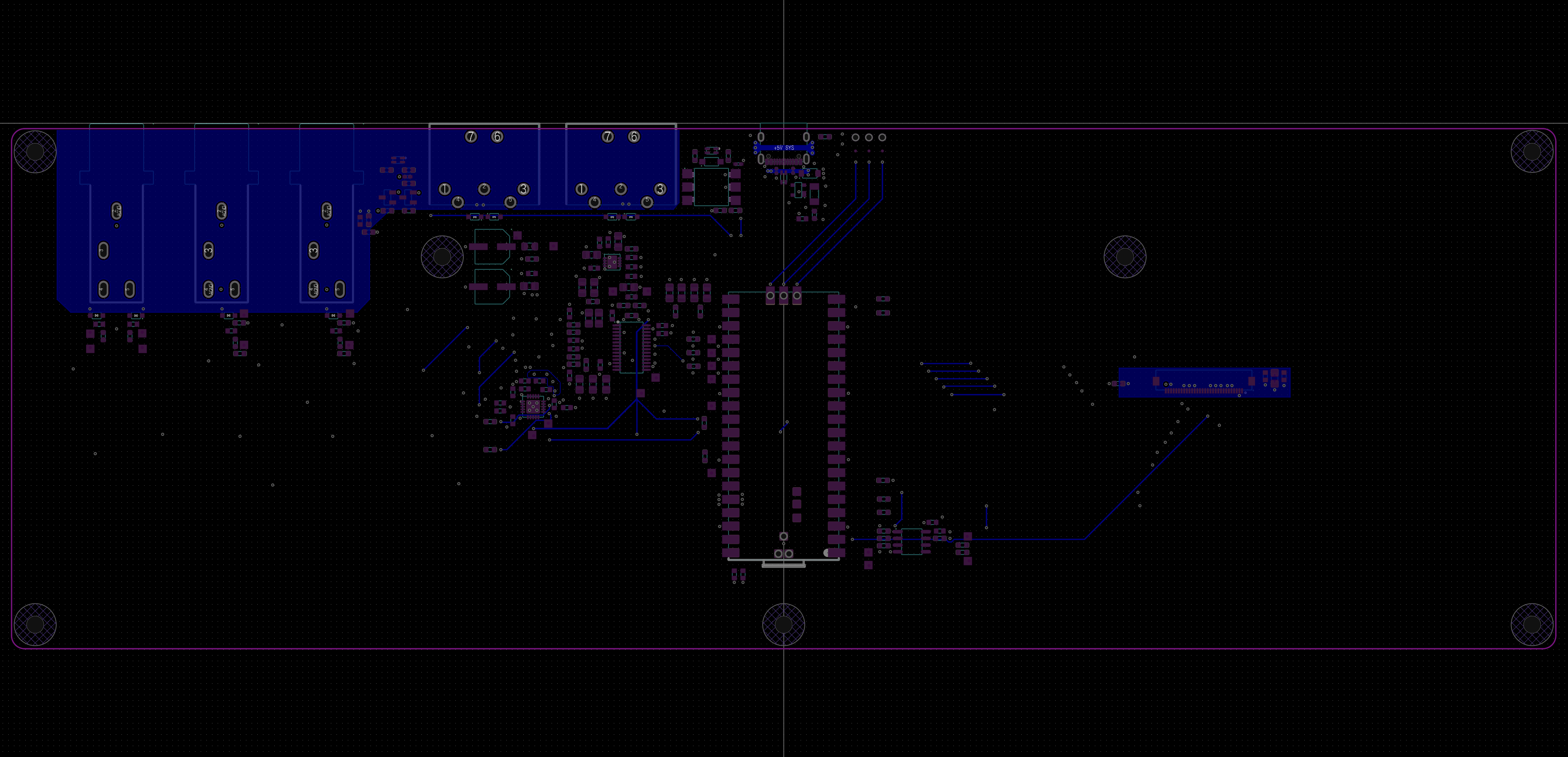
This revision focuses on refining the audio power and signal layout, separating AGND/DGND domains, and finalizing the analog output paths (DAC → Line / Phones).
- Introduced a local `+5V_AUDIO_Analog` plane on Inner2 exclusively for the headphone amp (TPA6130A2).
- This simplified routing and reduced coupling around the charge pump region.
- Maintained at least 2mm clearance between the charge pump loop (CAPP/CAPM/VNEG) and all power traces.
- Ensured continuous AGND on Inner1, no necks or splits.
With all components placed and DRC passing cleanly, the PCB measures 294 × 99 mm — fitting perfectly inside the planned 296.6 mm internal width enclosure.
It was a demanding phase, but the layout came together faster than I expected — a relief, honestly. There are still rough edges to refine, and I can already see places that could be improved with more polish. Fortunately, there’s no rush. I’ll take as much time as needed to make it right.
Discussions
Become a Hackaday.io Member
Create an account to leave a comment. Already have an account? Log In.