 Hiroyuki OYAMA
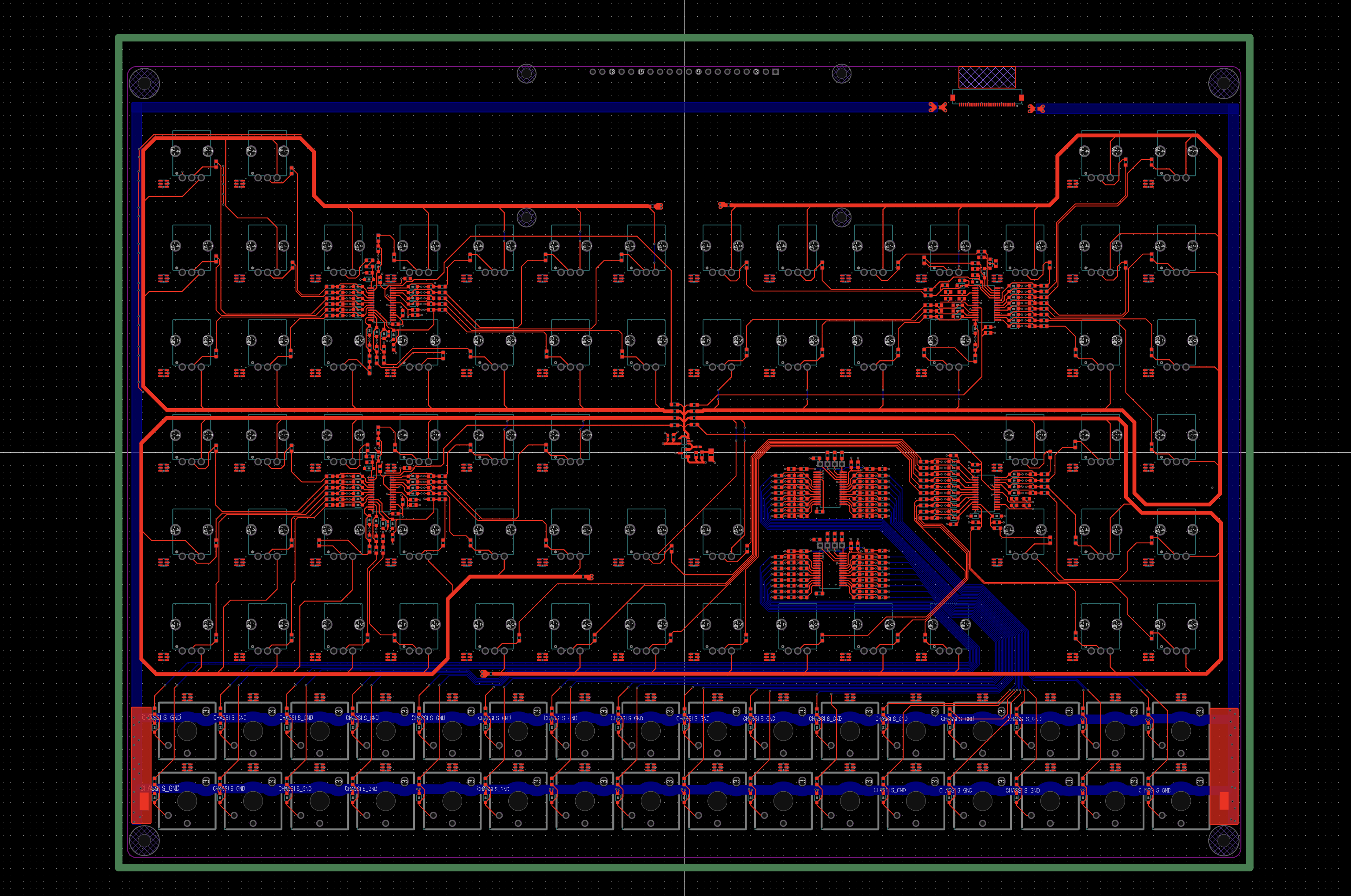
The UI board has finally passed its steepest mountain —
all potentiometer, ADC, key switch, and I/O expander connections are now fully routed.
This section was particularly challenging:
- 64 analog potentiometers (each with low-pass and reference routing)
- 32 independent key inputs through two MCP23S17 expanders
- Integrated ESD paths, shielding traces, and shared ground planes
- 96 LEDs to coexist in the same grid
After many iterations, I managed to fit everything while preserving:
- Continuous ground on inner layer (L2)
- Reserved space for LED horizontal buses (Bottom layer)
Next, I’ll start routing LED data and power (L3) —
but with the entire input system already verified, I feel the design has crossed its biggest hurdle.
Discussions
Become a Hackaday.io Member
Create an account to leave a comment. Already have an account? Log In.