 Hiroyuki OYAMA
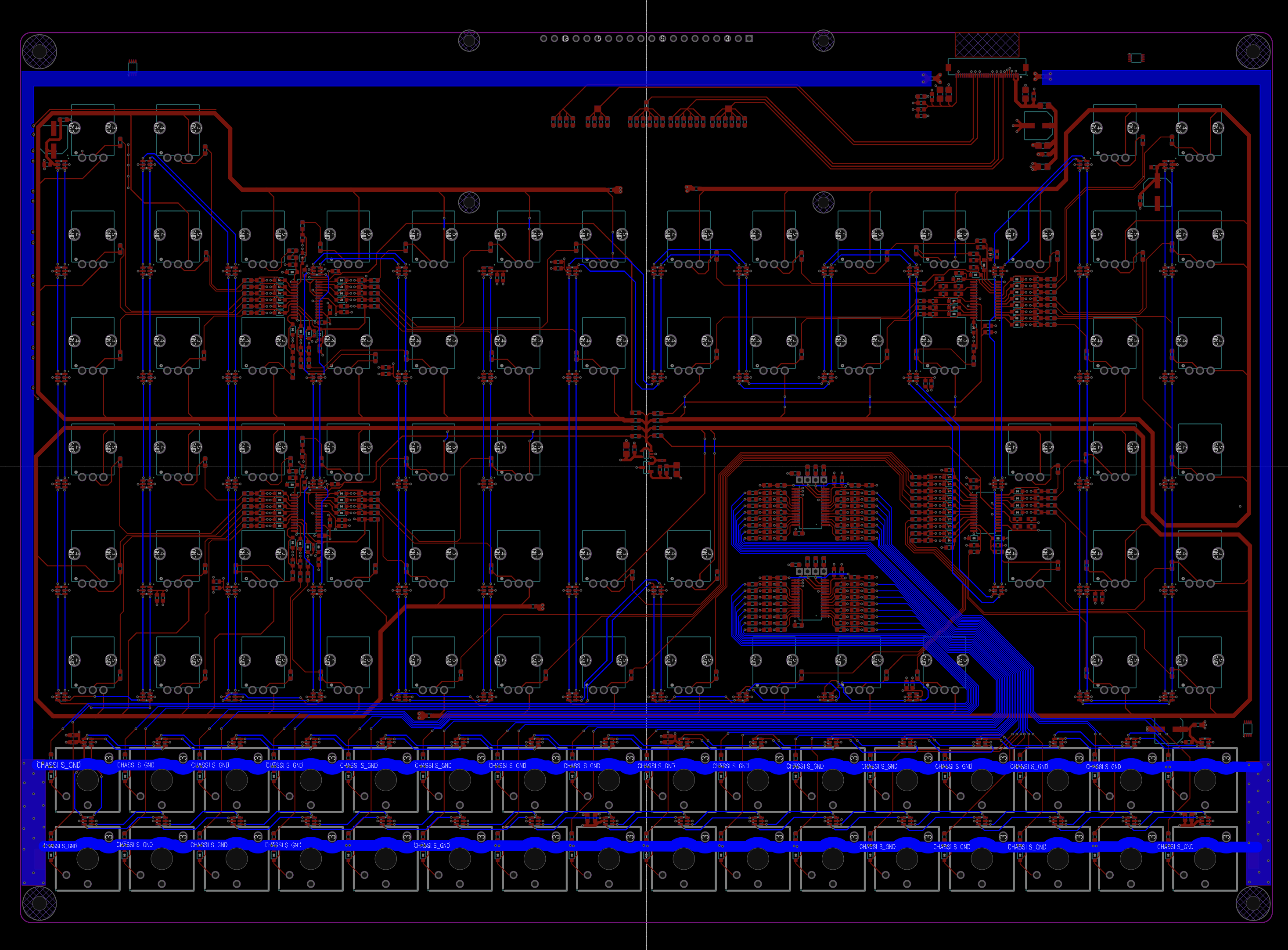
Today I completed routing all 96 LEDs on the Darśana UI board, including those for the key switches.
The southern “dead-end” section turned out to be the biggest challenge, but all LED chains are now fully connected. With this, all display-related circuits — LEDs and OLED — are now wired and ready for verification.
To prevent interference with the analog input section (ADC / VREF), the LED layout follows a layered structure:- LED signal lines are routed on the bottom layer,
- Analog VREF and potentiometer wiper lines remain on the top layer,
- and a continuous L2 GND plane is placed between them to minimize coupling.
This approach allowed me to arrange 64 potentiometers, 32 key switches, and 96 LEDs in a high-density layout while keeping the overall circuit structure well organized.
The next steps will be:- placing LED drivers at the origins of each LED chain,
- completing the SPI routing (SCK / TX / RX / CS), and
- refining the inner2 power plane for +3V3_UI_D, +3V3_UI_A, and +5V_UI_LED.
Now, every visual element on the UI board finally has a clear path for light to travel.
Discussions
Become a Hackaday.io Member
Create an account to leave a comment. Already have an account? Log In.