 Hiroyuki OYAMA
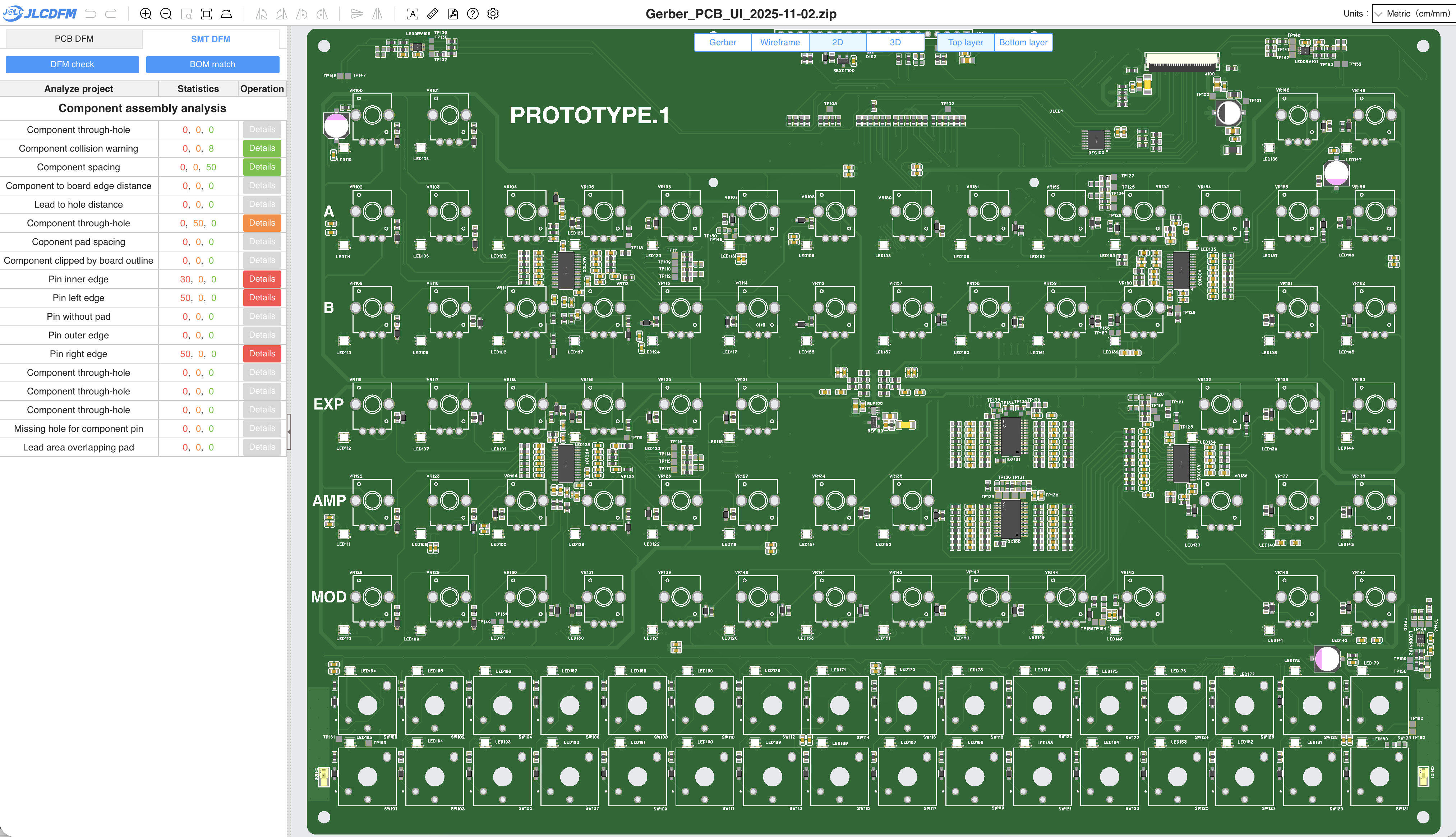
I ran exhaustive checks using JLCPCB’s online DFM tool and revised the design until it was fully manufacturable for both PCB and SMT assembly.
Some traces were redrawn to flow more naturally, some issues were patched or adjusted with minor compromises, and a few alignments had to be intentionally broken to make things fit.
All major risk points (Dangers) have been cleared, and the remaining Warnings are within acceptable limits for production.
After going through this process, the overall routing feels cleaner, and the entire circuit design now looks more coherent and balanced.
Discussions
Become a Hackaday.io Member
Create an account to leave a comment. Already have an account? Log In.