 Jesus Angel Martinez Mendoza
Summary
A 16×2 LCD controller built entirely from multiplexers and logic gates — no microcontroller, no firmware. This project demonstrates how 8 multiplexers (4:1) can be configured as a ROM to execute a complete LCD initialization sequence and later allow user input in ASCII through simple pushbuttons. It is a working proof that digital logic alone can replicate the core functions of a microcontroller.

Inspiration
Every tutorial on LCDs starts with an Arduino. But what if you removed it — completely?
That question led me to an unusual challenge: build a self-contained LCD controller without using any programmable device. The idea evolved through several experimental phases — from random number generators and asynchronous counters to the creation of a custom instruction memory made entirely of multiplexers.
The result: a logic-based LCD driver that initializes the display automatically and then allows users to type any ASCII character through a hardware keyboard.
How It Works
1. System Overview
The project is divided into six functional blocks:

| Subsystem | Function |
|---|---|
| Clock Generator (NE555) | Produces pulses for synchronization. |
| Instruction Memory (8×MUX 4:1) | Acts as ROM to send 4 preprogrammed LCD instructions. |
| Control Unit (Counters + Logic) | Sequences the instructions and switches to manual mode. |
| Keyboard Interface (Pushbuttons + Logic) | Allows user to input ASCII data manually. |
| Display Driver (Logic OR + LCD) | Routes either automatic or user data to the LCD. |
| Power & Brightness Control (MOSFETs) | Regulates contrast and backlight with pushbuttons. |
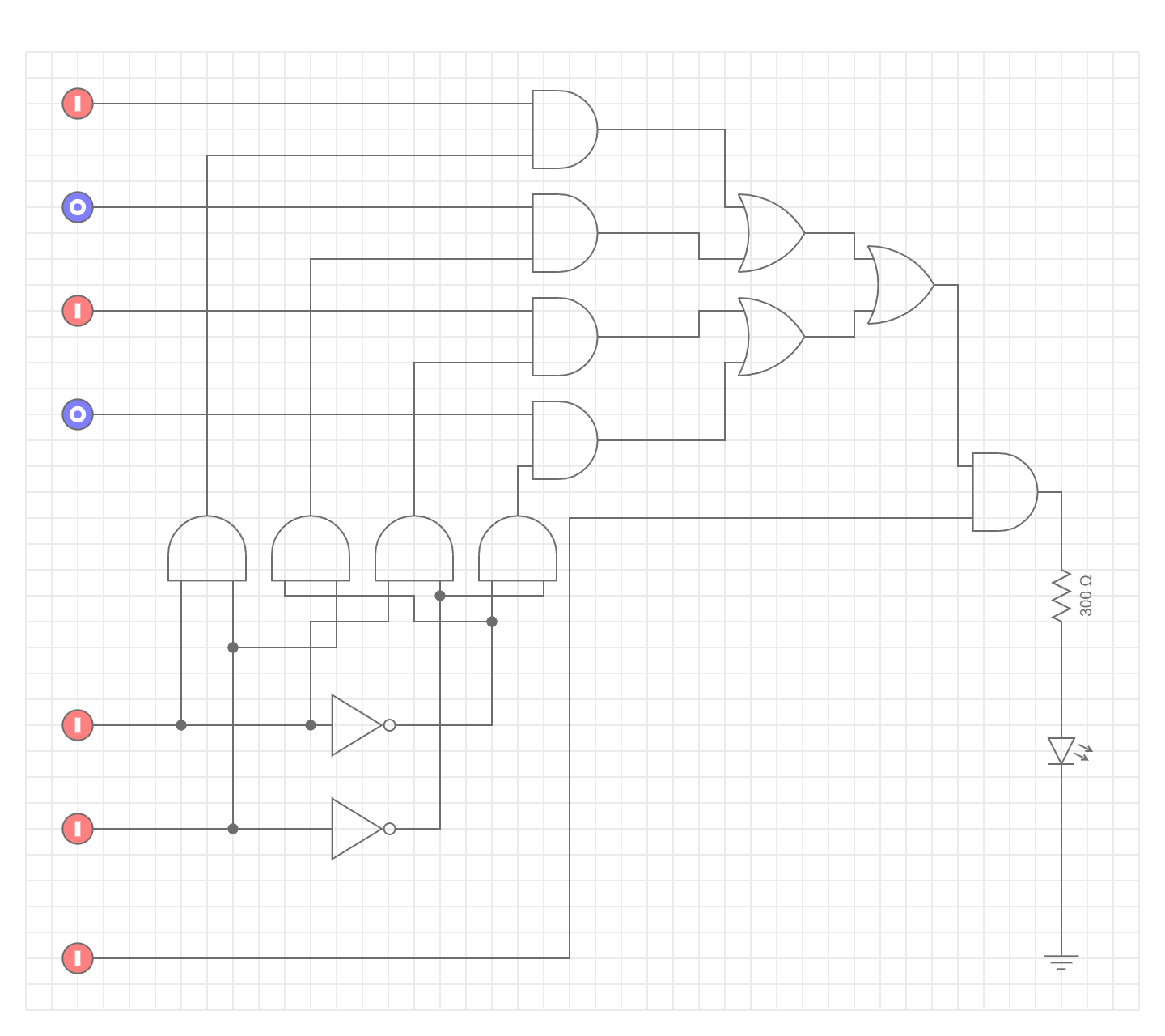
2. Instruction Memory (Abusing Multiplexers)
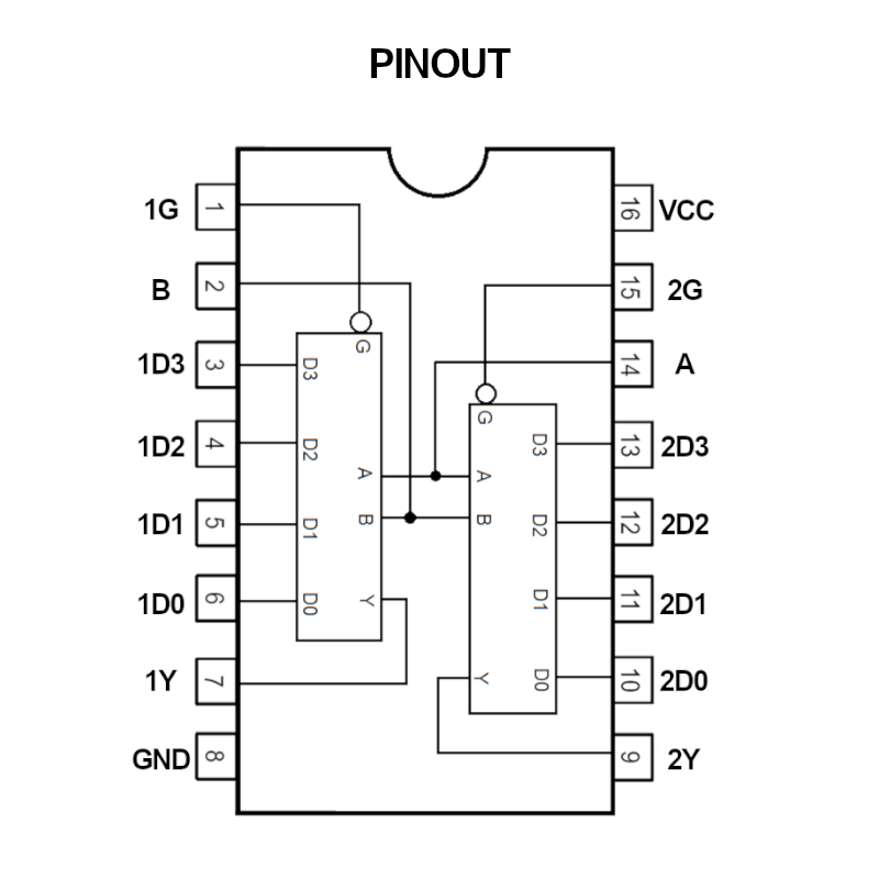
At the heart of the project lies a memory made from 8 multiplexers 4:1 (74LS153).
Each multiplexer stores one bit of a 4-word ROM. Two control lines (S<sub>0</sub>, S<sub>1</sub>)
select which instruction is active:
| S1 | S0 | D7 D6 D5 D4 D3 D2 D1 D0 | Instruction |
|---|---|---|---|
| 0 | 0 | 0 0 1 1 0 0 0 0 | Configure 8-bit mode |
| 0 | 1 | 0 0 1 1 1 0 0 0 | Enable 2 lines |
| 1 | 0 | 0 0 0 0 1 1 1 1 | Show cursor |
| 1 | 1 | 0 0 0 0 0 0 0 1 | Clear display |
Each combination of (S<sub>1</sub>, S<sub>0</sub>) triggers a unique 8-bit word that the LCD interprets as a valid command.
This structure transforms the MUXes into a hardware ROM.
3. Control Logic (Sequencing the Memory)
The sequence through the four instructions is handled by a 4-bit binary counter (74LS193).
The counter cycles through 00 → 01 → 10 → 11, feeding the selection inputs of all MUXes simultaneously.
When the counter finishes the sequence, a control signal EN switches the system into user mode.
Truth Table for Memory Sequencing
| Time (t) | S1 | S0 | EN (Active) | Description |
|---|---|---|---|---|
| 0 | 0 | 0 | 1 | Send first instruction |
| 1 | 0 | 1 | 1 | Send second instruction |
| 2 | 1 | 0 | 1 | Send third instruction |
| 3 | 1 | 1 | 1 | Send fourth instruction |
| 4 | – | – | 0 | Stop automatic mode |
Once EN = 0, the control is transferred to the keyboard circuit.
4. Keyboard Interface (ASCII Entry)
The keyboard consists of pushbuttons representing binary bits (D0–D7) and an ENTER key. The user sets the desired 8-bit ASCII code manually and presses ENTER to send it to the display.

Example: To send the character ‘8’ (ASCII 56, binary 0111000):
| D7 | D6 | D5 | D4 | D3 | D2 | D1 | D0 |
|---|---|---|---|---|---|---|---|
| 0 | 1 | 1 | 1 | 0 | 0 | 0 | 0 |
Pressing ENTER triggers a short pulse equivalent to the LCD “Enable” command.
5. Dual Data Input
A logic OR gate merges signals from both the automatic memory and the user keyboard. During initialization, only the ROM is active. Once setup is complete, the MUX memory is disabled, allowing user inputs to flow freely into the LCD pins.
This transition mimics the firmware “setup() → loop()” structure found in microcontrollers — but achieved with nothing but hardware.
6. Power, Brightness, and Contrast Control
To make the system self-contained, a custom voltage regulator and brightness/contrast controller were built using MOSFETs and pushbuttons. Each MOSFET acts as a variable resistor controlled through small pulses, adjusting the current through the LCD backlight or VO pin.
| Control | Function | Element |
|---|---|---|
| Bright+ / Bright− | Backlight regulation | IRFZ44N |
| Contrast+ / Contrast− | Adjust display contrast | IRFZ44N |
| Power Switch | Main supply control | Transformer 12 V → Regulators 5 V, 12 V |
This adds autonomy and a clean aesthetic — no Arduino, no external PSU modules.
Truth Tables and Timing
Memory Operation (Example MUX)
| S1 | S0 | Output |
|---|---|---|
| 0 | 0 | C0 |
| 0 | 1 | C1 |
| 1 | 0 | C2 |
| 1 | 1 | C3 |
This behavior is exploited to map instruction bytes, effectively turning address lines into program counters.
Timing Sequence
t0 – Power ON → Counter Reset
t1 – ROM[0] executes (LCD Function Set)
t2 – ROM[1] executes (Enable Lines)
t3 – ROM[2] executes (Cursor On)
t4 – ROM[3] executes (Clear Display)
t5 – Switch to manual mode
t6+ – User inputs ASCII data manually
This timeline was validated both in simulation (Tinkercad / Proteus) and in physical hardware.

What Makes It Special
- No microcontroller or programmable logic
- Fully autonomous LCD initialization
- User input through pure hardware
- Custom-made instruction memory from multiplexers
- Educational value in digital architecture and control design
- Beautifully visual — you can see every bit move
This design redefines how we think of “code”: here, logic gates are the program.
Lessons Learned
- Multiplexers can act as both selectors and data containers.
- The limits of “hardware-only computing” go further than expected.
- Timing mismatches and propagation delays must be treated as design constraints, similar to clock cycles in CPUs.
- Hardware can think, given enough organization.
Future Improvements
- Expand memory to 8×8 words to allow full-screen ASCII messages.
- Implement EEPROM-style reprogrammability with jumpers or DIP switches.
- Add a seven-segment output for debugging current instruction.
- Create a transparent acrylic enclosure with labeled blocks for exhibition.
- Integrate a small logic analyzer LED array to show signal propagation.
Technical Summary
| Component | Description | Qty |
|---|---|---|
| 74LS153 | Dual 4:1 Multiplexer | 8 |
| 74LS193 | 4-bit Up/Down Counter | 2 |
| 74LS273 | 8-bit Register | 1 |
| NE555 | Clock Pulse Generator | 1 |
| IRFZ44N | MOSFET Brightness/Contrast Control | 2 |
| LCD 16×2 | Output Device | 1 |
| Pushbuttons | ASCII Input | 12 |
| Logic Gates (AND, OR, NOT) | Control Signals | Various |
Conclusion
The μMUX Display Controller proves that programmable behavior can emerge from non-programmable components. By pushing multiplexers beyond their intended use, I built a functional, fully automatic LCD driver that bridges the gap between digital logic and computation — without writing a single line of code.
It’s not just a circuit. It’s an homage to the essence of computation — where logic itself becomes language.
— Jesús Ángel Martínez Mendoza