 Clara Hobbs
I started looking at ways to make the power/data splitter described in the last post, and the situation didn't look good. I didn't want the side that plugs into the PD Buddy Sink to have a female connector because I don't know how e-marked cables would like being chained together. However, all the male connectors I found either had to be reflowed, which I'm not capable of doing at home, or require 0.8 mm PCBs, which I can't find a way to get for under $50 in under 3 weeks. I really don't want to spend that much or wait that long, so I had to think of another way. I thought about hacking apart two USB cables, but again, I'm not sure how e-markers would like that. What to do?
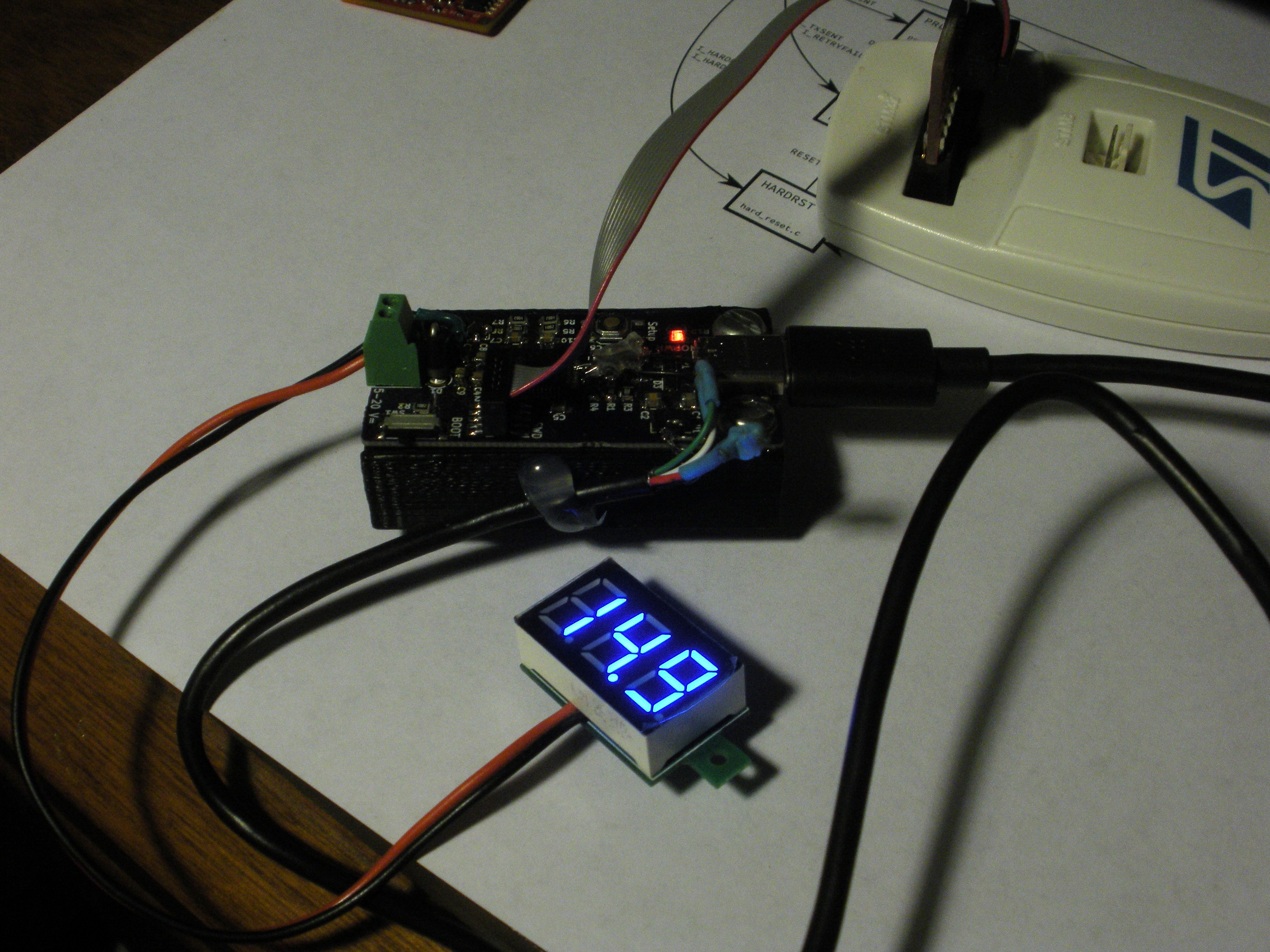
Well, I have two v0.1 PCBs lying around unused. They've already been hacked on quite a bit to fix the schematic errors in that version, so a bit more ugliness wouldn't hurt anyone. I decided to cut the USB D+/- traces and solder a USB cable's GND, D+, and D- wires to the board to have separate data and power connections. After some tricky fine-pitch soldering, the ugly board came to life!
After some testing, I've concluded that the problem I observed yesterday was in fact the fault of the Asus USB 3.1 UPD Panel, not the PD Buddy Sink. This is welcome news, since it means I don't have a weird bug to track down and fix. Now I get to go back to developing new features instead of quietly worrying!
I still might design a power/data splitter board, since it could be useful to people other than myself. But since I personally have no urgent need for one, I'll probably only make it if someone out there asks me to.
Discussions
Become a Hackaday.io Member
Create an account to leave a comment. Already have an account? Log In.