electronicsworkshops
Introduction
Modern electronic design must prioritize effective and adaptable power management, particularly for battery-operated devices where the input voltage varies greatly throughout discharge cycles. The design and execution of a Single-Ended Primary Inductor Converter (SEPIC) based on the MT3608, a low-cost, high-frequency boost converter integrated circuit, are shown in this project. By adding a linked inductor and a Schottky diode, the MT3608 may be set up as a SEPIC even though it is not its native architecture. This creates a converter that can generate a steady output voltage that can be adjusted to be greater, lower, or equal to the input voltage.
For Full Project:
https://electronicsworkshops.com/sepic-dc-dc-converter-using-the-mt3608-boost/

Objective
To design and build a versatile, wide-input-range DC-DC converter capable of maintaining a stable output voltage that can be either higher or lower than the input voltage, using the cost-effective MT3608 boost converter IC in a SEPIC configuration.
Key Specifications
- Input Voltage Range: 2.5V to 16V
- Output Voltage Range: 3.3V to 12V (adjustable)
- Maximum Output Current: Up to 1.5A (depending on Vin-Vout differential)
- Efficiency Target: 80-90>#/li###
- Primary Application: Battery-powered systems where input voltage varies above and below the required output voltage
How a SEPIC works?
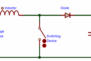
A SEPIC (Single-Ended Primary Inductor Converter) functions by utilizing two inductors (L1 and L2) and a coupling capacitor (C_couple) to move energy from the input to the output in two separate phases. When the internal switch (e.g., in the MT3608) is ON, the input voltage charges L1, capturing energy in its magnetic field, while at the same time the coupling capacitor discharges, transferring its accumulated energy into L2. When the switch is OFF, the collapsing magnetic fields of the two inductors work together, forward-biasing the output diode and enabling the combined energy from L1 and L2 to charge the output capacitor and supply the load. This distinctive push-pull mechanism via the coupling capacitor allows for the output voltage to be accurately controlled at a level that can be either higher or lower than the input voltage, while ensuring a non-inverting output and shared ground with the input.
Why the MT3608 alone is not a SEPIC controller?
The MT3608 is not capable of functioning as a SEPIC controller because it is specifically designed to operate as a boost (step-up) converter; its internal control circuitry and power switch configuration are exclusively built for elevating voltage from the input to the output. A SEPIC (Single-Ended Primary Inductor Converter) requires the use of two inductors (or a coupled inductor) along with a coupling capacitor to facilitate both step-up and step-down capabilities, with energy transfer being managed in a manner distinct from that of a boost converter. The MT3608 does not possess the necessary control logic and feedback compensation to effectively regulate voltage when the input voltage is higher than that of the output — it can only function properly when the output voltage exceeds the input. Attempting to configure it in a SEPIC manner would lead to instability, inadequate regulation, or potential circuit failure.
Circuit Diagram


Circuit overview
This circuit uses the MT3608 IC (U3) to boost (step up) a DC input voltage to a higher output voltage.
- The input voltage (VIN) is applied at the right side through a slide switch (PWR1) that turns the converter on or off.
- The output voltage (VOUT) appears on the left side.
- Key components: L1, D2, C1–C4, R1–R2, and the MT3608 itself form the boost converter’s power and feedback network.
a. Inductor L1 (22 µH, 3 A)
- L1 is the main boost inductor.
- When the MT3608’s internal switch (connected to pin 1, SW) turns on, current builds up in L1.
- When the switch turns off, the inductor’s...
 hesam.moshiri