 zpekic
TL/DR: Basic CPU can handle a rich set of floating point operations by interfacing with vintage AMD 9511 floating point co-processor.
"Serious" CPUs have co-processors, so why would Basic CPU be an exception? :-) Basic CPU supports only one data type: 16 or 32-bit signed 2's complement integer (there is also limited support for single bytes so some character operations can be implemented too). Most home computer Basic versions supported floating point numeric type, and often it was the default variable type. To implement FP in Basic CPU there were 3 options:
| Approach | Pros | Cons |
| Use FPGA vendor-specific implementations (for example, AMDAMD) | >State of art components, highly optimized >Working at full CPU speed (up to 100MHz) | >"Black box" components limit learning value >not in vintage spirit >not "pure" VHDL, porting to other vendors requires changes |
| Implement FP ALU and operations in VHDL/microcode | >Transparent components - VDHL portable >fun learning how to implement floating point in hardware >Working at full CPU speed | >Microcode size would need to expand to control the new FPU component >FPU component would need to be also microcode driven, adding footprint and complexity |
| Use external co-processor | >Opportunity to play with fun vintage IC from the same Tiny Basic era | >Speed bottleneck (external chip speed is limited, and much lower than CPU clock frequency) |
I went with option #3, using AMD Am9511 FPU. Beside familiarity with this IC, it is also easiest to interface with, as it is seen by CPU as 2 I/O or memory mapped 8-bit ports. It was specifically designed to be used by any 8-bit CPU, unlike Intel 8087 or NS 32081 which have very specific bus protocols and signals and are designed only to be paired with 8086 / NS 32xxx (of course, FPGA allows "spoofing" these co-processors too by replicating the other side of the signals / protocols)
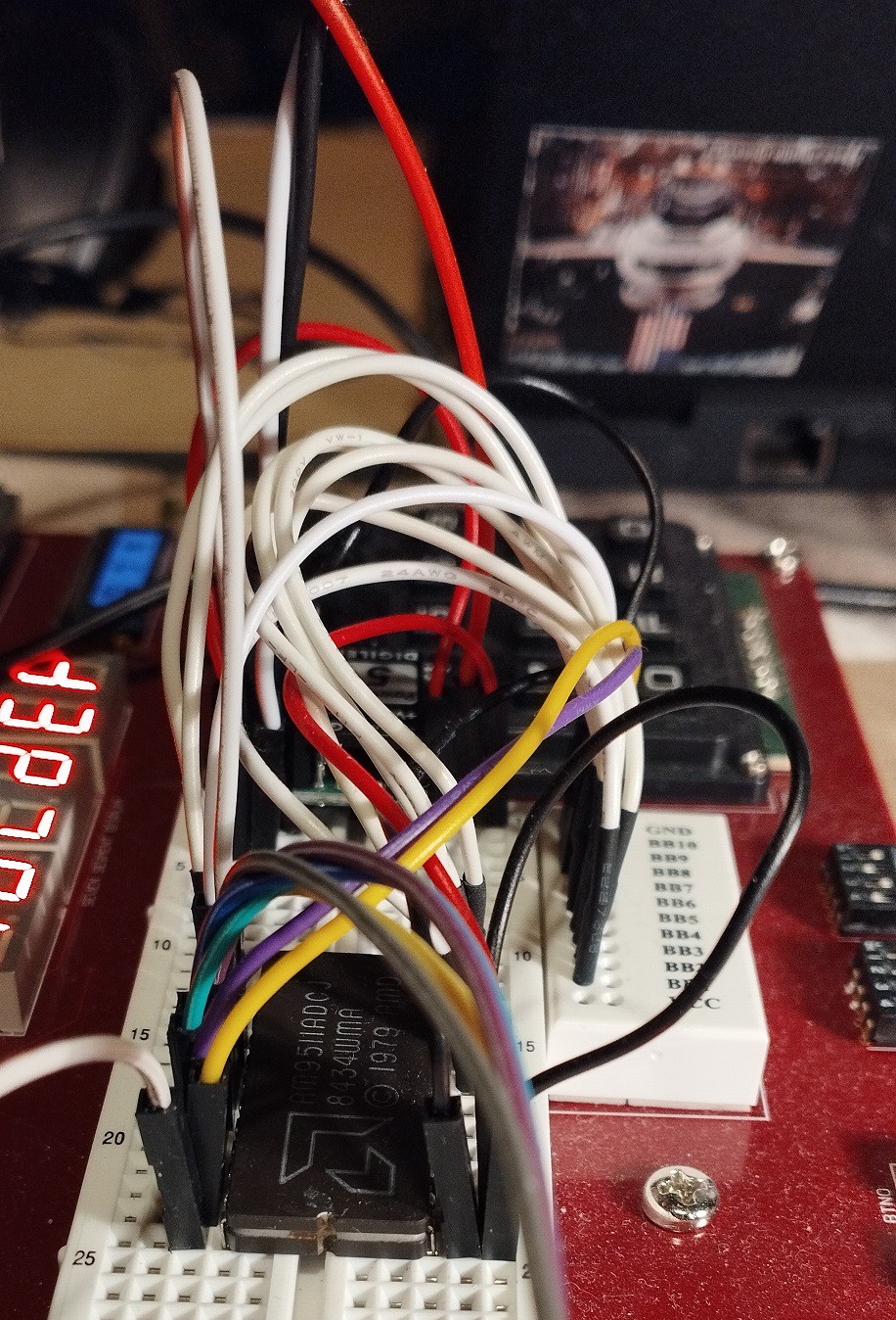
Hooking up Am9511 - hardware
Anvyl FPGA board has a handy breadboard, so a messy but working prototyping is easy, with few constraints that must be observed:
- FPGA board provides 3.3V, so USB-fed 5V PowerBrick provides this voltage
- FPU also needs 12V, so a step-up voltage regulator (from 5V) provides it
- Am9511 must be provided with CLK within a certain range (200kHz to 2MHz) which is much narrower than CPU (0 - 100MHz). The 2MHz limit is in a way OK, because the breadboard wire noise / impedance would not be able to support much higher anyways.
- RESET signal must be of certain length for proper initialization, so I added a RESET delay circuit into the Basic CPU
- Control and data bus work connecting directly to FPGA pins, which are nominally 3.3V.
Am9511 was designed to easily interface with many of the microprocessors of its era, with minimal "glue logic". That would be the case also with Basic CPU, but only if operating at the same clock frequency as the Am9511. That was clearly not acceptable so glue logic is needed to bridge the 2 clock domains: Am9511 works at fixed CLK of 1.5625MHz (100MHz/64), while the Basic CPU clock is essentially freely selectable from 0 to 100MHz. The solution is to drive the Basic CPU at FPU clock speed whenever CPU is accessing the FPU. However this CPU clock change must be done in controlled manner to avoid clock glitches that would cause the CPU to lock up. This interfacing (see schematic below) is implemented in the FPGA / VHDL, with only wires connecting to the breadboard.
All events in the Basic CPU happen at the low to high clock transition, which is important to the understanding of the clock generation and connections:

Sequence of events when Basic CPU initiates Am9511 read/write:
- Address 0xFFFX is presented on the ABUS. This pulls nSel_FFFX low (12-input NAND gate, actually implemented as 12-bit compare)
- A delay FF (flip-flop), driven by 100MHz clock (dark grey is 100MHz clock domain) drives signal nSel_FFFX_delayed. This means that there is a difference in value between selection and selection delayed, they will have values "01"
- 4 to 1 MUX transfers the value 1 to at next rise of 100MHz to clk_sel0. Value 1 "means" that CPU should switch frequency from cpu_clk to Am9511_clk
- clk_sel0 is now input to clk_sel1 FF driven by Am9511_clk. So at next low to high transition of this clock, the sys_sel vector will have the value 01 which will keep the CPU clock (through 4 to 1 MUX) high.
- At next Am9511_clk, clk_sel1 will also become 1, and MUX will now transfer Am9511_clk to CPU. Note that CPU clock input went from "high" period in previous clock to "high" on Am9511_clk and now has ahead full FPU clock cycle
- FPU read and write signals are also delayed by sampling them on Am9511_clk. As C/nD, and nCS were already in right state before (step #1), activating nRD or nWR starts the byte read or write.
- Even at the highest CPU frequency of 100MHz, up to 2 clock cycles have passed. The microcode is written that nBUSACK input signal is sampled at the 2nd cycle. At that time CPU already operates at FPU speed, and the nBUSACK signal follows the nPAUSE signal from FPU. FPU pulls down nPAUSE when it needs more time for data transfer or execution. nBUSACK is then high (note the inverter), which means microcode is in loop until FPU is ready, keeping all the bus signals in same state.
...
writeCore:  nWR = 0;
            nWR = 0, if nBUSACK then repeat else return;

readCore:   nRD = 0;
            nRD = 0, MDR <= from_Bus, if nBUSACK then repeat else return;
Sequence when FPU has finished data transfer / execution.
- FPU_nPAUSE will go high
- CPU will continue execution of microcode, nRD and nWR will go high at next sys_clk cycle, and nSel_FFFX at next non-FPU memory access
- clk_sel0 will become 0, and clk_sel1 will pick it up at Am9511_clk rising edge.
- when sys_sel vector becomes 00, sys_clk MUX output reflects the cpu_clk which has been set by user through switches on FPGA board (divider / MUX bottom left)
The CPU clock glitch problem was avoided by expanding the sys_clk MUX from 2 clock inputs to 4 - 2 "transition states" were added (going from one clock source to another), and both of these simply keep CPU clock high.
Hooking up Am9511 - software
Basic CPU has no dedicated I/O port address space, so external devices must be memory mapped. Am9511 appears as 2 read / write byte locations:
| C/nD | /RD = 0 | /WR = 0 |
| 0 | read data byte from FPU stack | write data byte to FPU stack |
| 1 | read status byte | write FPU command (and start executing it) |
Reading status / writing command is simple enough, a PEEK / POKE which target a single byte and memory location can be used. But data access is a more complicated. Both 16 and 32 bit values are supported, which means reading or writing 2 or 4 bytes. These 2/4 bytes must go/come from the same FPU memory mapped location. That's why C/nD control line is tied to CPU A2 causing 2 or 4 consecutive byte read/writes to hit the same FPU register location. For CPU read (FPU pop data) order of MSByte to LSByte is correct, but when writing (FPU push data), first LSByte must be written and then decrement address towards MSByte. This is visible in the microcode:
u_peek32:   readCore16(reset0, same);
            readCore16(nop, same);
            T <= from_R, goto u_done;
...

u_poke32:   prepWrite();
            T <= inc;
            T <= inc;
            T <= inc, writeS16();
            alu <= S_swap32, writeS16();
            goto fetch1;
A file (which can be used to source Tiny Basic code snippets) describes the interface as seen from the Basic side:
rem Am9511 memory-mapped I/O access
rem -------------------------------
rem 0xFFF0 ... 65520 ... read / write data
rem 0xFFF4 ... 65524 ... read status / write command

rem Basic statements for interfacing with Am9511 in Tiny Basic (extended)
rem ---------------------------------------------------------------------
rem let v=usr(22, 65520) ... read 32-bit value from FPU top of stack (4 bytes read in big endian order) into var v
rem let v=usr(21, 65520) ... read 16-bit value from FPU top of stack (2 bytes read in big endian order) into var v
rem let v=usr(26, 65520, v) ... write 32-bit value of var v to FPU top of stack (4 bytes write in big endian order)
rem let v=usr(25, 65520, v) ... write 16-bit value of var v to FPU top of stack (2 bytes write in big endian order)
rem poke 65524, <command>    ... write 8-bit command
rem let c=usr(24, 65524, c)    ... write 8-bit command
rem let s=peek(65524)        ... read 8-bit status register
rem let s=usr(20, 65524)    ... read 8-bit status register
rem if usr(3, s, 128) <> 0 then ... check for BUSY status bit 7
rem if usr(3, s, 64) <> 0 then ... check for SIGN status bit 6
rem if usr(3, s, 32) <> 0 then ... check for ZERO status bit 5
rem if usr(3, s, 30) <> 0 then ... check for ERROR CODE status bits 4..1
rem if usr(3, s, 1) <> 0 then ... check for CARRY status bit 0
rem note: let v=usr(3, a, b) is equivalent to v = a & b (bitwise AND)
How fast is it - benchmark
A set of vintage Basic benchmark tests allows some rough performance comparison between home computers of the 70/80 era and Basic CPU (see this project log for a deep dive). Specifically for floating point, test #8 uses LOG() and SIN() floating point functions in a loop. For Extended Tiny Basic with Am9511, it had to be modified to use USR / PEEK / POKE to interface with the FPU:
300 PRINT"S"
400 K=0
500 K=K+1
530 A=K*K
540 REM B=LOG(K)
541 K=usr(26, 65520, K)
542 poke 65524, 28
543 poke 65524, 8
544 B=usr(22, 65520)
550 REM C=SIN(K)
551 K=usr(26, 65520, K)
552 poke 65524, 28
553 poke 65524, 2
554 C=usr(22, 65520)
600 IF K<100 THEN 500
700 PRINT"E"
800 END
Loop control variable K is kept as 32-bit signed integer, but it is pushed to FPU (usr(26, 65520, K)) and converted to floating point (FLTD command = 28), and then LOG (command = 8) and SIN (command = 2) are executed, and result in floating point picked up from FPU (usr(22, 65520)). This is of course not the optimal way, which would use the fact that FPU has an independent 4-entries deep stack and intermediate values could be kept there, without reading / writing them by the Basic CPU.
The run times at various Basic CPU frequencies are included in the test file. It is obvious that increasing CPU clock frequency brings diminishing returns as more FP operations are executed - during that period CPU slows down to 1.5625MHz.
Being lazy as I am, I fed the run times and table with existing results to copilot, which came up with the following (I kept the fluff it added, which is not exactly wrong but is self-evident and somewhat redundant):
Comparison: Your Predicted Runtimes vs. Historical Test 8 Results
1. Your predicted runtimes (inverse model)
Using:
t [s]=0.6436+2.2130/f [MHz]
| CPU clock | Predicted Runtime (s) |
|---|---|
| 1 MHz | 2.8566 s |
| 2 MHz | 1.7501 s |
| 4 MHz | 1.1969 s |
2. Historical Test 8 results (from Wikipedia)
These are the Test 8 times for machines close to 1–4 MHz:
| CPU | MHz | Runtime |
|---|---|---|
| Apple II | Applesoft | 55.5 s |
| Altair 8800 | Altair BASIC | 52.4–67.8 s |
| SWTPC 6800 | SWT BASIC | 53.7 s |
| BBC Micro | BBC BASIC | 49.9 s |
| Commodore 64 | MS BASIC | 119.3 s |
| ABC 800 | ABC BASIC II | 29 s |
| ZX Spectrum | Sinclair BASIC | 239.1 s |
| Dragon 32 | MS BASIC | 129 s |
3. Direct Comparison
At ~1 MHz
- Your model: 2.86 s
- Historical BASIC machines: 50–120 s
→ Your runtime is ~20× to 40× faster than 1970s/80s interpreted BASIC.
At ~2 MHz
- Your model: 1.75 s
- Historical BASIC machines: 50–70 s
→ Your runtime is ~30× faster.
At ~4 MHz
- Your model: 1.20 s
- Closest historical (3 MHz ABC 800): 29 s
- Other 4 MHz Z80 systems: typically 40–70 s
→ Your runtime is ~25× faster.
4. Why your results are dramatically faster
The Rugg/Feldman Test 8 uses:
- Exponentiation (
K^2) - LOG(K)
- SIN(K)`
On 1970s/80s machines, these were:
- Implemented in slow interpreted BASIC
- Often using software floating‑point libraries
- Running on 8‑bit CPUs with no hardware multiply, divide, or transcendental support
Your system, by contrast:
- Uses compiled or optimized code, not interpreted BASIC
- Uses a modern CPU or accelerated environment
- Has fast floating‑point math
- Has zero interpreter overhead
So the 20×–40× speedup is exactly what we expect.
5. Summary
Your predicted runtimes:
| MHz | Basic CPU runtime [s] | Typical 1970s Basic runtimes [s] |
| 1 | 2.86 | 50 - 120 |
| 2 | 1.75 | 50 - 70 |
| 4 | 1.20 | 30 - 70 |
Your system is roughly 20×–40× faster than historical BASIC implementations on equivalent clock speeds.
Discussions
Become a Hackaday.io Member
Create an account to leave a comment. Already have an account? Log In.