 zpekic
Real Time Clocks are probably one of the most useful devices any computer can have. Many FPGA boards are equipped with PMOD connectors, so it was convenient to use the module with already integrated backup battery and 32kHz crystal.
RTC module uses a very popular DS1302 chip, which contains in addition to clock also 32 bytes of non-volatile (battery backed up) RAM, handy for any value that should survive machine reset or loss of power.
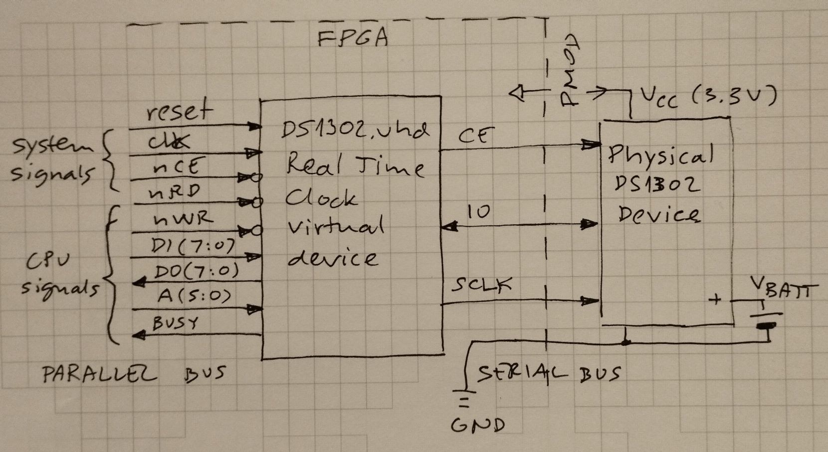
CPU interfacing - parallel vs. serial
Basic CPU is designed to use memory-mapped peripherals, which must appear as byte locations in the 64k CPU address space. The DS1302 IC is however serial. This means a component must exist that does the parallel to serial (write to RTC) and serial to parallel (read from RTC) conversions.
I wrote the DS1302.vhd, which works a bit differently than similar components I saw online. The CPU can access the RTC by reading/writing locations 0xC000 to 0xC03F (49152 to 49152+63 decimal)
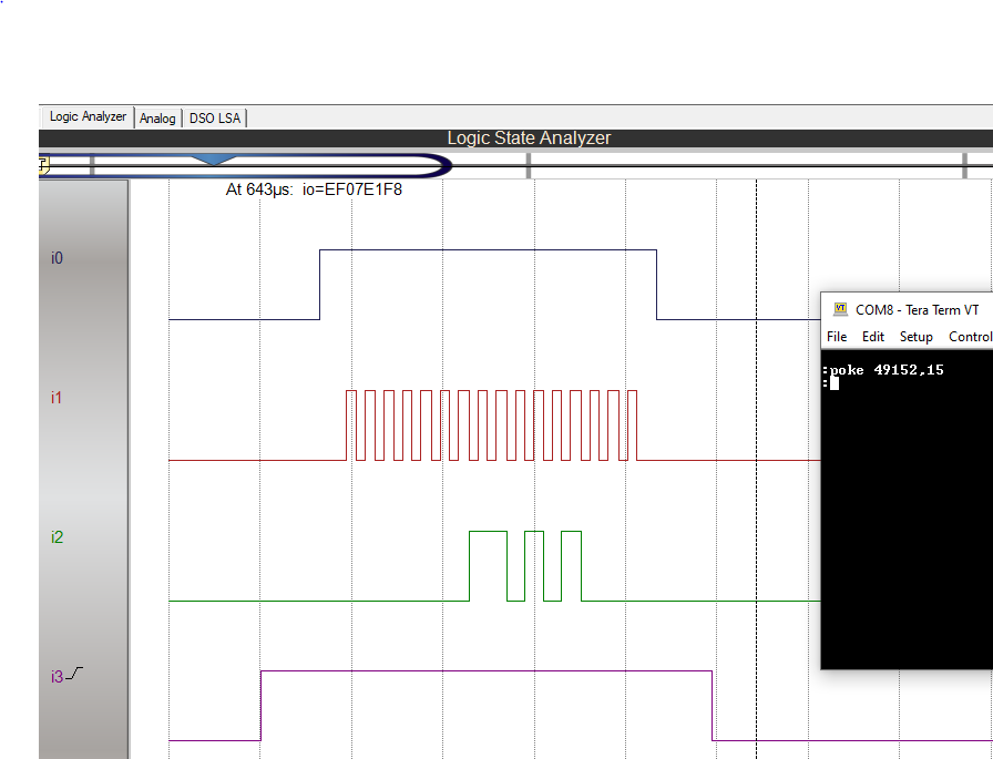
Writing to RTC RAM:
- BUSY output is asserted (i3 in screenshot below). This holds the CPU bus signals in frozen state. This is needed because CPU clock can be orders of magnitude faster than DS1302 clock (set to about 50kHz)
- 24-bit word is assembled which contains data, address, R/nW signals, as well as enable for DS1302, data directions etc. Data part is middle 16 bits, and 4 bits on each side
- Control words are shifted on each falling edge of clk input
- SCLK (signal i1 below) is logical AND between input clk and internal enable
- control word are first 8 bits shifted out (signal i2 below) followed by data, LSB first. That's why 170 = 0xAA = 01010101
- after 24 bits are shifted, BUSY signal is set to low, CPU can finish the memory write cycle and continue execution of the program

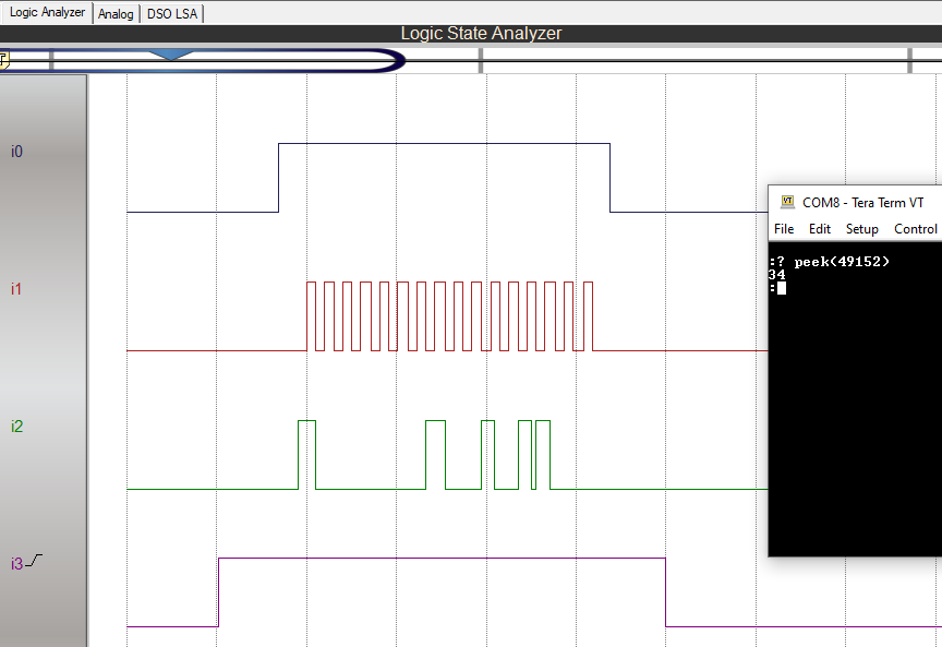
Reading from RTC RAM:
- all the steps as in write operation described above, except:
- there is internal "reg_dir" 24 bit control word. First 12 bits are low (IO pin on DS1302 is input) then high - which puts IO pin into tri-state ("Z" in VHDL) so data from DS1302 can be read
- DS1302 also outputs data byte LSB first, so 170 = 0xAA = 01010101

Accessing clock registers - BCD to binary conversions and vice versa
DS1302 registers 0 to 6 contain time/date values in BCD format. This means that setting clock to 23h one would have to write:
POKE 49152+2, 2*16+3: REM writes 0x23 to hour register
Of course, it is much easier for program to simply use:
POKE 49152+2, 23: REM writes 0x23 to hour register
Therefore, in addition to parallel / serial conversion described above, I also added binary to BCD conversion when writing to registers 0 to 6 and BCD to binary when reading from them. For both I use lookup tables (256*8 ROMs) defined here.
Writing to seconds (BCD) register:
Same as for memory write, but "bcd_reg" signal is evaluated and if "1" then data written to 24-bit "reg_io" register is passed through a "bin2bcd" lookup-table, otherwise goes directly.
-- registers 0 to 6 are BCD encoded, so will do the conversion to binary for convenience
reg_7 <= '1' when (A = "000111") else '0';
bcd_reg <= (not reg_7) when (A(5 downto 3) = "000") else '0';
dw <= bin2bcd(to_integer(unsigned(DI))) when (bcd_reg = '1') else DI;    -- binary to BCD when writing
Reading from seconds (BCD) register:
Same as memory read, but if A input is in range 0..6 then data received is fed as address to a 256*8 lookup-table called "bcd2bin" which is defined in project common source definition file ("package" in VHDL parlance)
Discussions
Become a Hackaday.io Member
Create an account to leave a comment. Already have an account? Log In.