 Vladimir Todorov

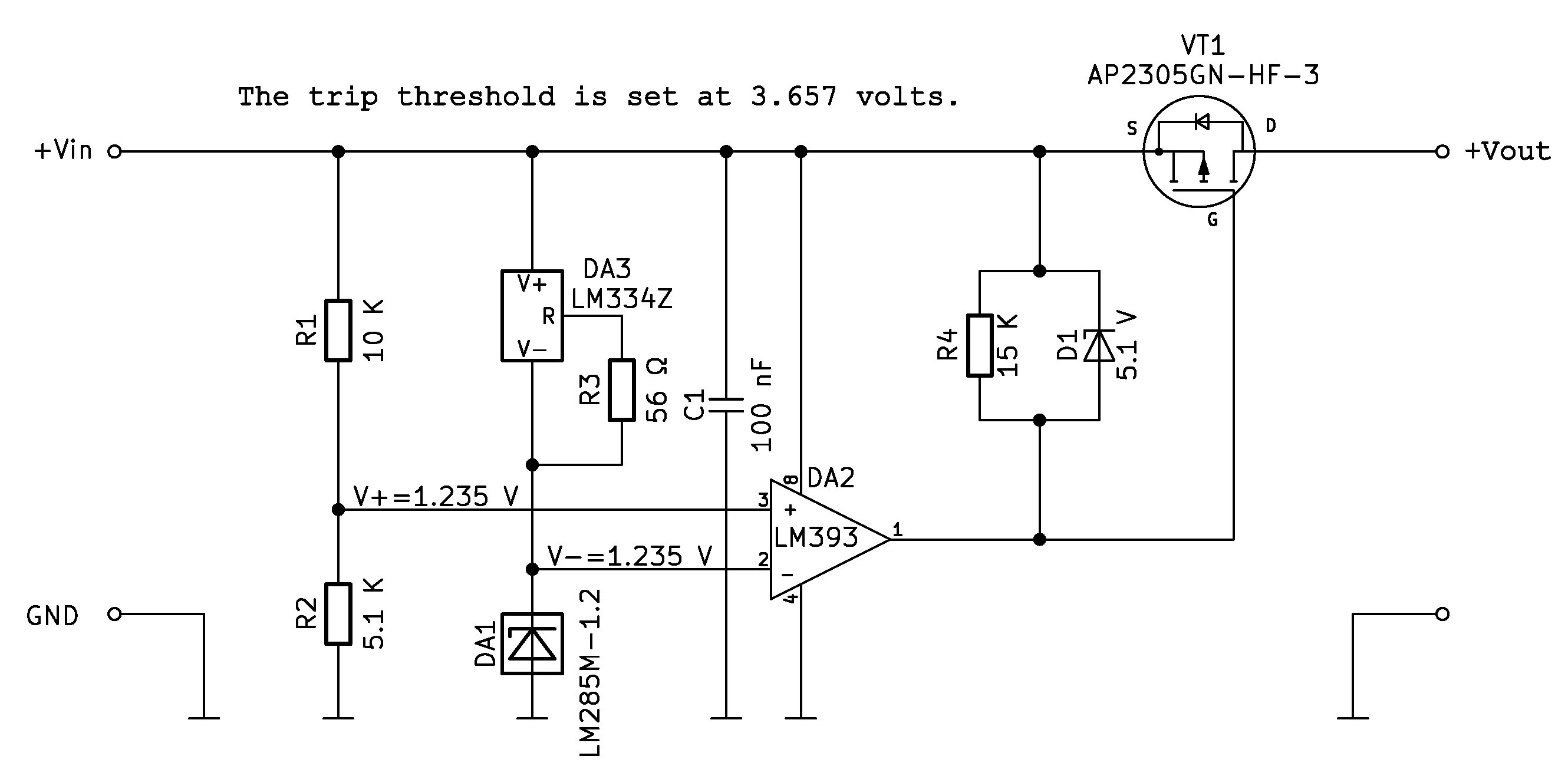
Overvoltage Protection Circuit Diagram
Circuit Description:
- Transistor VT1 functions as a series pass switch, controlling the power to the output.
- DA2 is a comparator with an open-collector output.
- DA1 is a precision voltage reference, set to 1.235 V.
- DA3, an Adjustable Current Source, provides a stable bias for DA1. While a simple resistor could be used here, the current source ensures more stable operation of the voltage reference.
- The input voltage is scaled down by the resistive divider R1 and R2.
- The voltage at the midpoint of the divider (across R2) is fed to the comparator DA2 and compared against the 1.235 V reference.
- Operation:
- If the voltage across R2 is below 1.235 V, the comparator's output is in a state that keeps VT1 turned ON.
- When the voltage across R2 exceeds 1.235 V, the comparator switches and VT1 is turned OFF, disconnecting the load.
For DA2: The maximum allowable supply voltage is 36 V.
For DA1: The maximum allowable supply voltage is 40 V.
For the transistor ( in this case, the AP2305GN-HF-3 ), the maximum voltage is -20 V.
Selection Challenge:
The transistor is the most difficult component to find. It needs to meet two key requirements simultaneously:
- Support a higher voltage.
- Have a very low threshold (turn-on) voltage.
For the AP2305GN-HF-3 , the gate threshold voltage ranges from -0.5 V to -1.6 V.
For a transistor like the DMG3401LSNQ :
The maximum allowable Drain-Source Voltage is -30 Volts.
The Gate Threshold Voltage is between -0.5 V and -1.3 V.
Perhaps some hysteresis should be added to the comparator. I leave this to the readers.
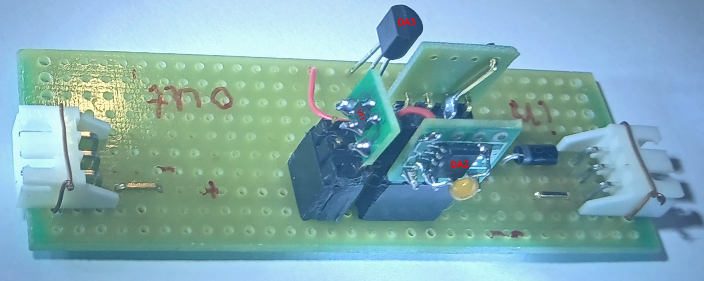
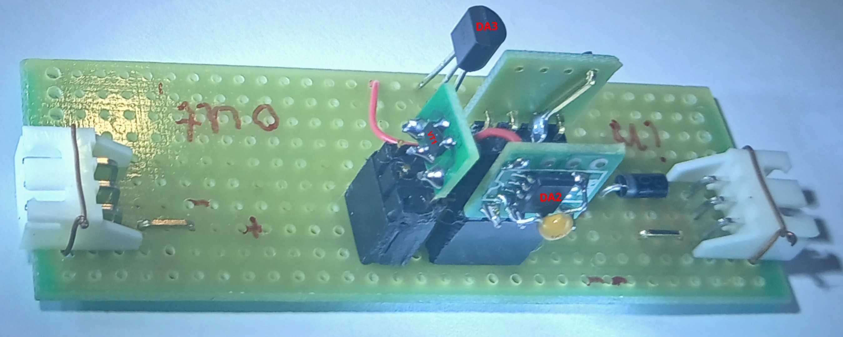
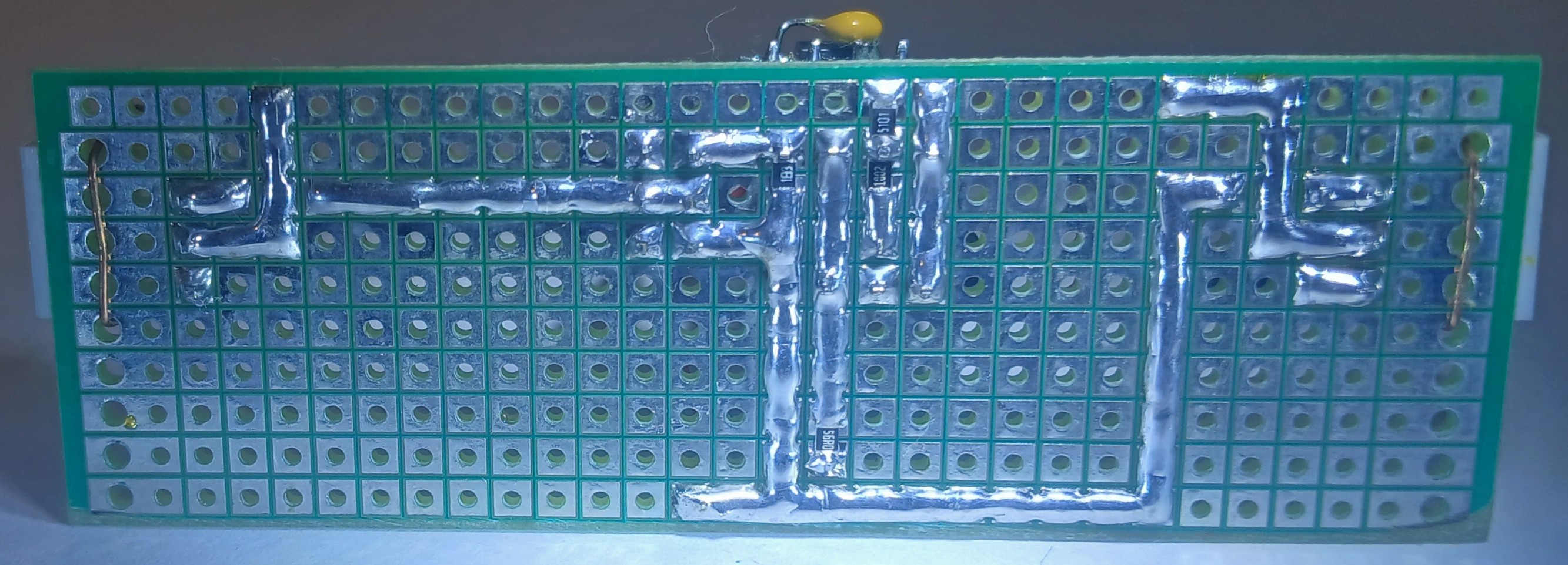
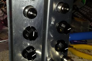
Some pictures :
 256byteram
 mircemk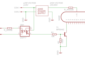
 Christoph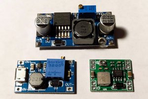
 Naman Chauhan