Leon
LeonSome time ago I needed a gift for a friend, who plays DND. So, the obvious choice was self-made dice in the favorite color of said friend. This is how my journey “dice making” began, hence this project.
I bought a cheap silicone mold for dice and epoxy colors from Amazon (d4 to d20). I already had epoxy resin at home. At my first try, the dice were already pretty good, but had too many bubbles inside. So, I spent a lot of time optimizing every step of casting them and finally got them as bubble free as possible. It wasn't until later that I learnt to get them completely bubble free I'd need a pressure pot (I still don't have one, though).
Next, I played with liquid cores in the dice, but that got boring fast.


I wanted to technologize the dice. First, I put wireless LEDs into them, but the light of those wasn't spreading enough. Because of that I added some LEDs to them, which led to some interesting structures. I am not sure if they are still completely fair, but it looks pretty so I won't change that.
But it was still not enough, surely, I could put more technical stuff into it.
And this is where I start:
The project in his humble beginnings
A big thank you to PCBway, as they sponsored this project and I wouldn't
have been able to do this without them. But more about that later.
What if the dice could automatically detect in which position they lay?
And then broadcast this to any device close enough to hear it?
My first instinct was to go with an ESP32, as it supports WiFi and Bluetooth, is relatively easy to set up and I have lots of experience using it.
The downside: it's too big.
If I cast this into the dice, there won't be any kind of connector to charge the battery, that's needed to power the ESP32. That’s why I chose wireless charging instead.
To regulate the voltage for the ESP, an LDO is needed. There had to be space for the sensors. I at least needed a 3-axis accelerometer, but the more sensors fit in there, the more functions the dice could have.
The ESPs start at 4x4mm footprint, I think, so they are already big. And with external periphery, like the antenna or the necessary crystal it's getting even “bigger”, without any external flash or RAM.
So, the ESP32 does not really fit for this project. I researched small microcontrollers with the ability for, at least, Bluetooth.
And I found one: the Renesas DA14531.
It has a size of 2x1.7mm and the ability to communicate via Bluetooth. Only downside: it only has an OTP memory. Once programmed, there is no updating code or changing it. Luckily, it can boot from SPI flash or I2C EEPROM.
It still needs a crystal and an antenna, but even combined those parts take less space than the bigger members of the Esp32 family, and for sure less than the smallest with periphery.
My 'far from perfect' design
As I had zero experience with the DA14531 or Renesas ICs in general, my design is sadly nowhere near perfection and contains some mistakes.
Most of the parts I chose were found by searching for whatever I needed (for example the crystal) on Mouser or Digikey and then filtering by size. The sensors were chosen with the help of ChatGPT. It helped me find out what would fit my project the best or makes the most sense when cast into resin (my PCB could also be used for other things than dice I guess).
I just wanted to cram as much functionality as possible into a very limited area. Which, in retrospective, may have been a mistake to begin with. But that's to be discussed later.
Power supply
After choosing the microcontroller, I focused on the power supply. I somehow had to get power into the dice, without a USB (or any other) connector. My first idea was using NFC and the power it provides. (Funfact: my first idea for this project was, to not use Bluetooth, but instead to use NFC.) I had an IC for this, which was a bit bigger than the DA14531, had like 100 pins in BGA package and needed a lot of fine-tuning with capacitors. Hence, I abandoned NFC. Then I thought back to the wireless LEDs, because they somehow needed to also get power without much fine-tuning and components. And it did indeed work:
There are ICs that can directly charge a battery with a simple coil and a very small number of capacitors. One of those parts is the LTC4124; I have not done the calculations for the perfect coil for this yet, but it works with the coil from the wireless LEDs, even if they are not perfect.
As batteries, I ordered a bunch of cheap 35mAh LiPos from AliExpress. Their dimensions are 5x10x10mm and they are functional. The only annoying thing about them is, that they don't seem to have inbuilt battery protection. That’s why I have to fit more components onto the PCB. I chose the GLF73610, as it was the smallest I could find.
Next on was the power regulation, as I didn’t want to feed the battery output directly to the DA14531. I think I could have simplified it, but I was not exactly sure about the power capabilities of the DA14531. Therefore, my motto was “better safe, than sorry”. So the TCR5FM30A entered my schematic.
The Memory
Now to the more interesting things:
The program memory. Aka an SPI flash.
There were a few requirements to be met here: It needed to have enough capacity. It needed to be battery friendly. It needed to be small. I investigated many different flashes, but in the end the MX25R8035FBHIH2 won my heart. It takes just around 0.8x1.2mm of space, has an SPI interface and enough capacity (1MB) for any code I’d want to run on a very complicated die. The only drawback: it is in a 8-WLSCP package, which would bite me a later on.
I also added an I2C EEPROM later. I had some free space on the PCB (I am not writing this in chronological order) and I2C already next to it. I wasn’t so sure what could fit there. First, I investigated a few sensors, but it was hard to find a sensor, that is around 1x1mm, has I2C and any practical usage in a die. I found a temperature sensor that fits those criterias, but I thought just a temperature sensor is boring and the DA14531 already includes a temperature sensor. I should have added an ADC with I2C interface to control the battery voltage (another mistake I made). But like that I could store stuff like character sheets outside program memory. Also, (but that was not planned) it kind of saved me some trouble.
The Sensors (finally)
All sensors or other periphery had to use I2C, as I wanted to save money, so, no Via in pads or very small vias. The DA14531 has some hard-to-reach pins underneath, which I wasn’t able to reach without the vias. There is a very limited number of available pins after having a SPI flash.
The first sensor I chose (as it was the main functionality of this project) was the Acceleration sensor.
There are a lot of sensors for this kind out there, starting with the very basic 3-axis acceleratormeter ADXL345 to the 9-axis super sensor combination BNO085. Unfortunately, those are too big. Once again, I asked myself: What is the smallest sensor I could find, that's still useable in such a project?
I found the BMA580 from Bosch sensortec to be very fitting. As it is smaller than the SPI flash, can be controlled via SPI or I2C, has up to two interrupt pins and can measure acceleration on 3-axis. It does also come in a 6-WLSCP package, so there is no assembly at home possible. Fortunately, it did not backfire like the SPI flash. I’ve often had positive experiences with Bosch sensors, which also helped me decide which one to choose.
The next sensor I included was a touch sensor. Because having some kind of input would be nice (for example when pairing with a device). I came back to the drawing board to get some ideas. The best I could come up with was a touch or proximity sensor. Anew, I investigated what is possible in as little space as I would want to use. In the beginning I wanted to have at least 12 touch channels (so each side of a D12 had its own touch input) but that was not possible in the small space I had. Soon after I found the company Azoteq and their touch sensors, which are very small. At first, I wanted to use one with 3 touch channels (like the IQS323001CSR) but they all come in an 11-WLSCP package, where one pin, that has to be connected, is in the middle and can't be brought out by a simple trace. It would have needed a via in pad.
That’s why I settled on a single channel touch sensor. I chose the IQS231B00000000CSR, which comes in an 8-WLSCP package and is as big as the chosen flash. The touch channel pin is routed to a pad, so I can solder on copper, that's used as input.
But my first decision for a 3-channel proximity sensor is still visible in the project. As the programmer I built for this has still 3 pogo pins for the 3 channels, instead of 1 that would be necessary now.
Anything not mentioned until here
One IC, that is not really a sensor, is a 3-channel LED controller, that's controllable by I2C. I had some space left and wanted to have some kind of feedback besides Bluetooth, so I used 3 LEDs. They aren’t placed perfectly as of right now, but they could be used (especially if I used more) to make cool light effects inside the dice. At the moment they are only orange. Though, there are some WS2812 LEDs, where each LED is only 1x1mm big, hence, a future iteration possibly could have a bunch of them on it.
Also, I have not said anything about the antenna so far: I chose a W3008C, which I’ve already used for different projects with the Esp32. I just roughly optimized the entire circuit around it. I have PCBs where I did not pay attention to this entire section and it worked perfectly with WiFi without fine-tuning anything, so, Bluetooth should not be a problem.
The Programmer
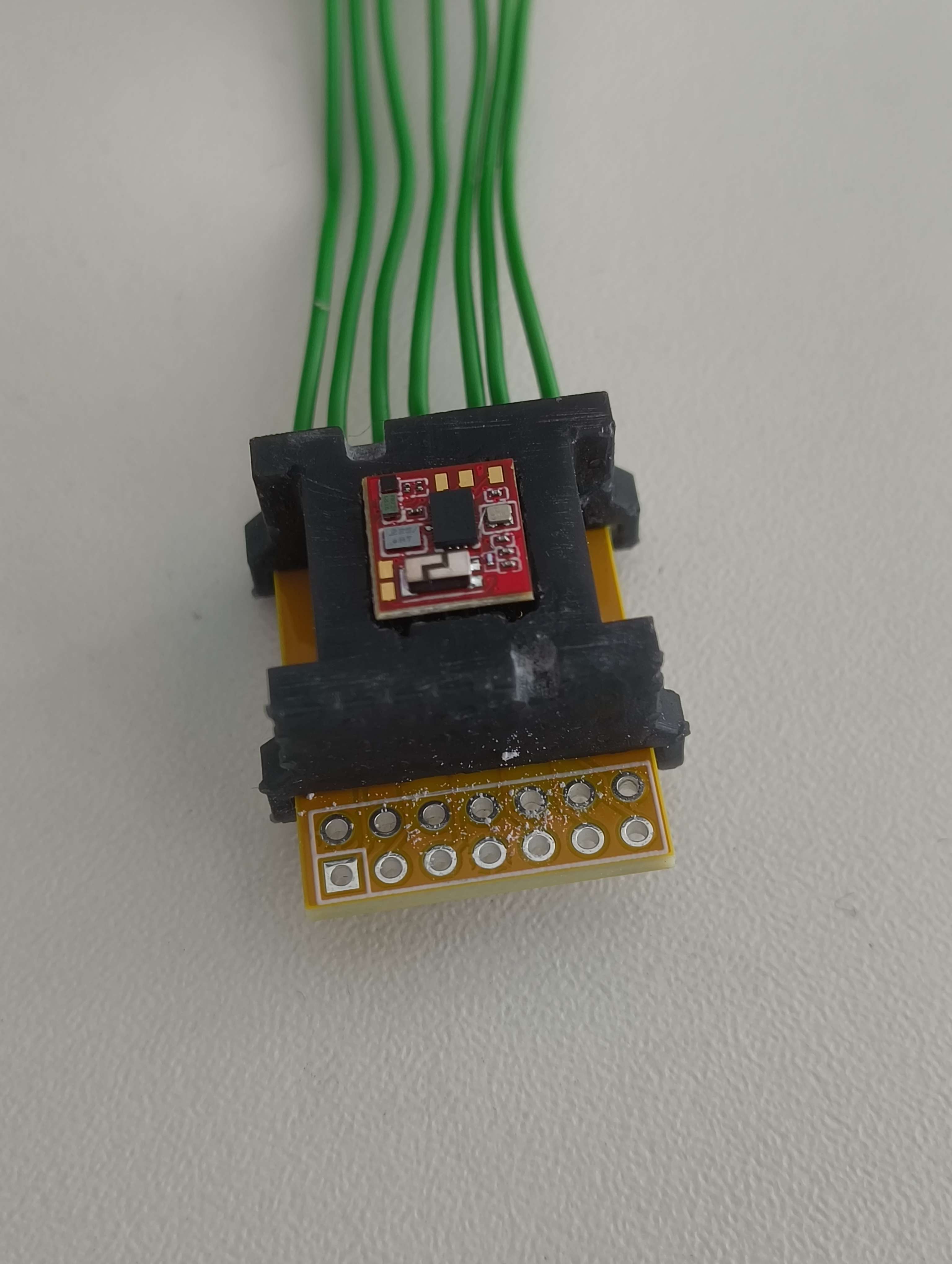
Because I wanted to be able to easily program and test the project, I designed two programmer PCBs as well as a 3d-printable enclosure. The PCB is put in and 12 pogo pins contact every bigger contact pad, including the power pins, the battery and the SWD interface.

The final PCB and a note of thanks to PCBway
As said before, I am very thankful to PCBway, as they supported my project so much. Thanks again for your patience, as you haven’t lost faith in me, even when the project hit roadblocks and everything got delayed.
The entire project was very expensive, especially because I needed a two-sided assembly to achieve the small size of the PCB. The whole PCB, with microcontroller, sensors, power management and everything else, is only 7.8x8.3mm big. Most capacitors and resistors are even too small to be seen, so I am impressed by how good they got assembled.
I think the whole thing is an absolute beauty and I am really happy how the PCBs turned out. Just look at it. It is so small and still got assembled successful. PCBway just outdid themself with this PCB.


I never ordered assembled PCBs from PCBway before, so I had no idea how the ordering process worked or what quality the product would turn out to have. Hence, I just clicked through the website and got a bunch of helpful information from their support (my conversation with them is something between 20 and 40 E-Mails deep), so everything worked out in the end.
The support of PCBway was helpful, as I made mistakes in the Gerber files, predominantly vias I put into a pad, even though I planned on not doing so. That was also the point in time, where I changed from a 3-channel proximity sensor to one channel.
If you want to try them out, you can use my link.
And even though I didn't use their 3D printing service in this project, I can just recommend it. I already used it in previous projects from time to time (just look at my project where I used it and wrote about it). Ordering is easy, turnaround is fast and their quality is outstanding.
The mistakes I made, improvements and future upgrades
Sometimes things just go wrong and sometimes I am just stupid
I think the biggest mistake I made was cramming so much things on the PCB without having a cheaper prototype first (even though the ones I ordered were not the ones I originally designed, because they would have been over 700 bucks for 5 PCBs). I had no experience using any of the components beforehand and still wanted to optimize everything for size.
Next thing I missed was entirely my stupidity:
For some reason I had one net in my schematic labeled 'SO' and confused it with the SI pin, which I need for the SWD interface. This made the programming a lot harder. The SI pin was "luckily" used for one of the pins of the SPI flash.
And this is the part where the small WLSCP package started to annoy me:
If the flash had little legs, I could have directly soldered onto them. If it was a QFN package, soldering a wire to the pad would have made it difficult, but still more doable than what I had to do: resolder the flash and solder a very tiny wire to one of the very small pins of the flash. I have no chance of putting back the flash, so no external program memory there.
This is when the EEPROM steps in to save me:
The DA14531 can boot from an external I2C EEPROM. So I could upload my code into this and still perform some software updates.
Unfortunately I knocked it of my test PCB while desoldering the flash. Yay, so no external program memory for my test PCB.


Now I had everything assembled. I abandoned the programmer after this mistake and soldered wires on every important interface. The programmer could simply not be used with another pin for the SWD interface, and I was to lazy to redesign the 3d Modell.
First, I tested the entire power section:
- I put 3V on the 3V line, nothing bursted into flames
- Connected the battery to the pins for the battery (I first had to short the pins of the battery protection IC as PCBway was not able to get ahold of them as part I chose had export restrictions)
- I soldered on a coil from one of the wireless LEDs
Each time it worked more or less. The coil was not optimized for the chip so I think there was not enough power for charging the battery. But the charging LED glowed dimly, which is a success to me.
Next I wanted to upload a simple test code, which would have shown the device to me via Bluetooth in the Renesas SmartBond app. I made everything ready ... Only to discover that my programmer for some reason wasn't recognised by my computer anymore. So I wasn't able to test any actual code on the chip so far, I already am ordering a new programmer and I will update this project when I am done with testing software.
Some improvements I already did or want to make
The first thing I changed was the confusion with the SI and the SO net, so programming is possible in the new design. For some reason this change was not safed so I have to redo this again.
As mentioned before, my actual first PCB included more sensors (temperature and hall), had 3 touch/proximity channel and a way more optimised routing, as it was a 6 layer PCB with buried vias. As it was to expensive, I simples down to a 4 layer board with less sensors and no buried bias.
Also, I learned that bigger footprints for resistors or capacitors could be good, because if one of those parts does need a repair, I won't be able to do that.
I plan on better placement of the LEDs, maybe even more LEDs, so the entire dice is lit up.
Also, adding a way to watch the battery percentage would be great, otherwise, the dice might stop functioning midgame without a warning.
The Future
I also thought about future "Add Ons".
I could add displays, either with I2C or displays with other interfaces.
Another idea would be a vibration motor. I am not sure what use this could have in a dice, but I am sure I could fit one into a dice.
Also, a smartphone app would be useful, for seeing what the dice rolled, statistical analysis, things like the battery percentage or for storing character sheets or something into the memory (I don't really know what use this would have, I have never played DND before). Also the app could be used to connect to the other players if you are playing virtually, so everyone can see what you threw.
One thing that sounds like a fun idea is pairing the dice with an Alexa (or another comparable device), so the Alexa says what number the dice landet on.
While writing this I got the idea to put an I2C NFC Chip into this die. With this I could for example simplify the bluetooth connection process. Or share information easily with the die. Maybe, updating the firmware via NFC would be possible.
The last thing (and probably the first I am gonna build when I finished the dice) is a case for the dice. With a slightly bigger battery, a wireless charging circuit inside and a way to detect the dice in the case to safe on battery while using the dice.
What else could be done with this PCB except over-engineered dice?
I have other ideas what could be done with this, but I won't evaluate the usefulness of those ideas:
- With a die with at least 10 sides, you could build a funky number pad, by rotating the dice onto the number you want to put in
- Some kind of cryptographic authenticator, like a YubiKey, just looking like a dice
- With additional or better fitting sensors this could be used as sensor board in places, where water tightness is required
I am open to get further ideas for future attachements or other use cases for this project.
Thanks to everyone who read till here. And thanks again to PCBway, they supported me a lot in this and some other project; you should totally check them out and order from them.
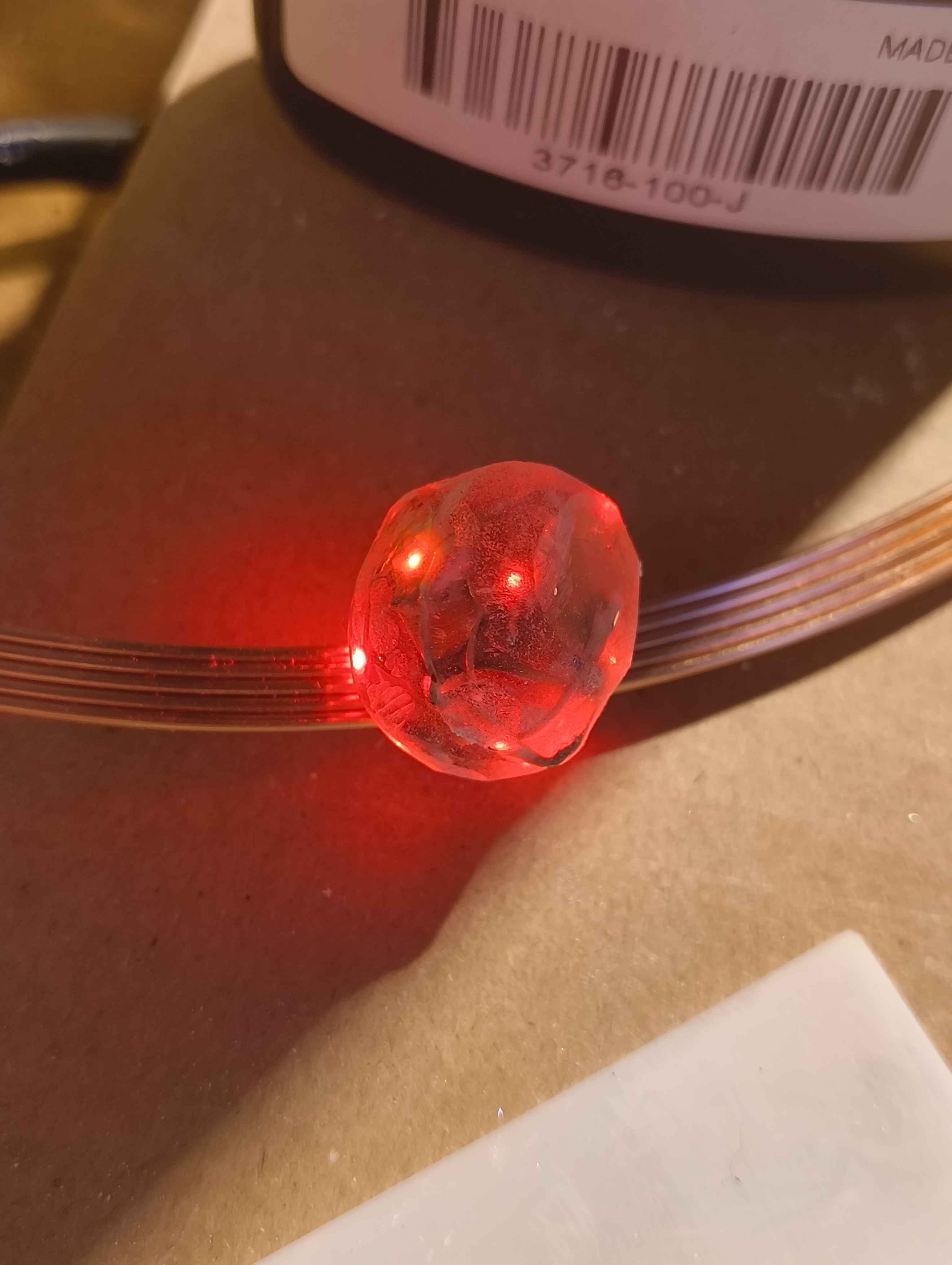
Random images of dice I made and from this project