 dev-lab
The Problem
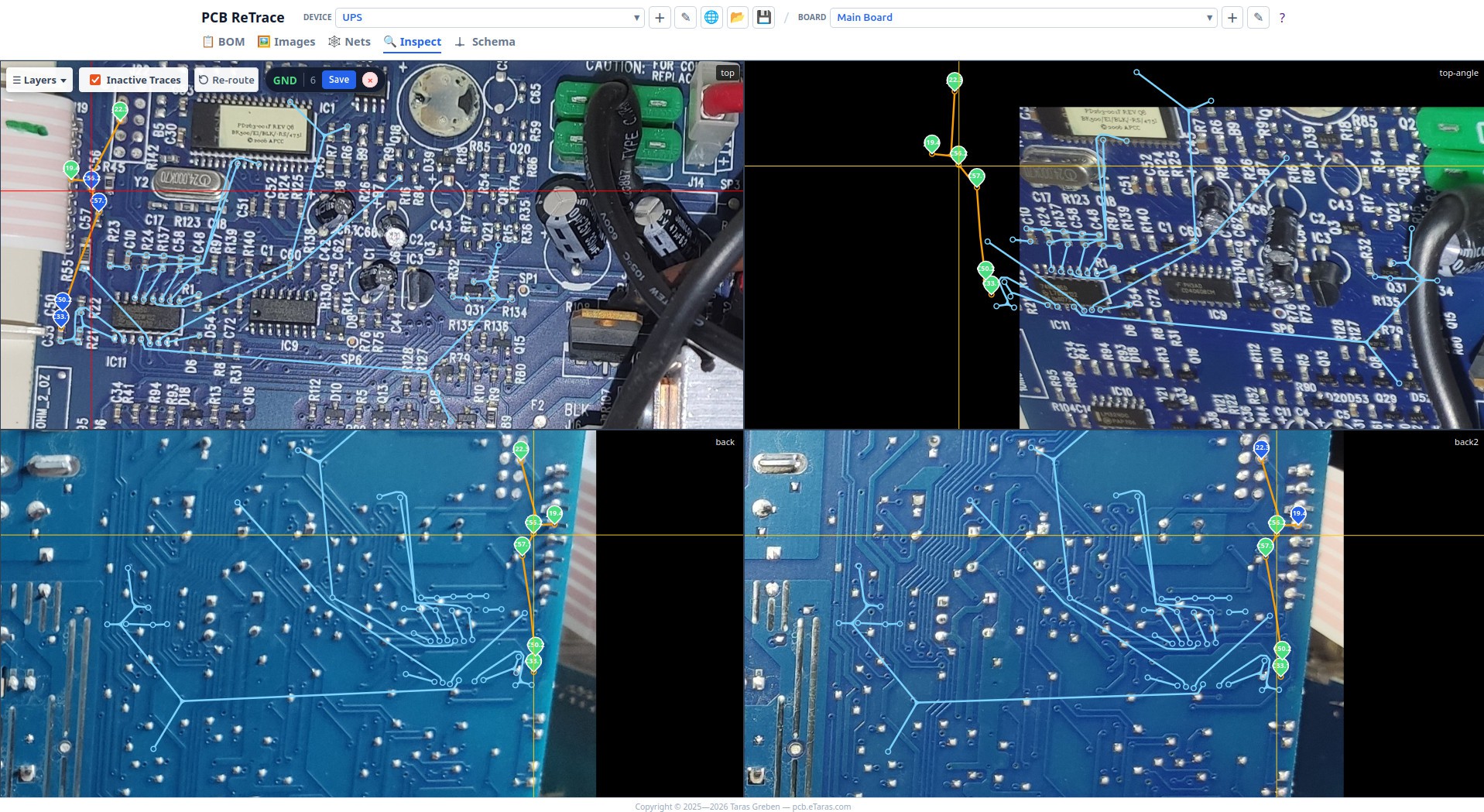
When repairing legacy hardware or analyzing a complex PCB without schematics, we often rely on high-resolution photos. But photos are static. You can't "click" a trace to see where it goes, and flipping between top and bottom board images mentally is error-prone. Existing software is often expensive, platform-locked, or relies on cloud services where you risk uploading sensitive IP.
The Solution: PCB ReTrace
PCB ReTrace is a browser-based suite designed to digitize and document physical circuit boards. It bridges the gap between a physical photo and a digital CAD file, running entirely in your browser using Local-first principles.
📺 Watch the Workflow Demo:
Key Features
🔒 100% Private & Offline Capable
- Zero Cloud Uploads: All images and project data are stored locally in your browser’s IndexedDB.
- Security: Perfect for proprietary or NDA-protected boards.
- Cross-Platform & Mobile Ready: Runs on Linux, Windows, macOS via Chrome/Edge/Firefox. Fully compatible with Android and iOS — perfect for taking to the workbench on a
tablet.
📸 Smart Image Stitching & X-Ray
- Auto-Alignment: Stitch multiple macro shots into a high-res map using WASM-powered computer vision.
- X-Ray Vision: Align Top and Bottom board images precisely. Trace vias and connections through the board views.
📝 Visual BOM Management
- Interactive Mapping: Click a component on the photo to add it to your BOM.
- Cross-Probing: Clicking a row in the BOM list instantly zooms to that component on the board.
- Live Editing: Add values, packages, and descriptions on the fly.
🕸️ Netlist Tracing & Export
- Draw Traces: Visually draw connections over your photos to define Nets.
- Smart Node Inspector: Finely tune pad and pin assignments with smart auto-suggestions for component naming and built-in pinout cheat sheets.
- KiCad Ready: Export your work as a verified Netlist for CAD recreation.
🗺️ Schema ReTrace (Built-in Schematic Generator) - NEW!
- Instant Schematic Generation: Move beyond raw netlists. Schema ReTrace turns your mapped components and traced nets into a readable visual schematic diagram.
- Seamless Integration: Your schematic updates directly alongside your board photos as you trace nets and assign pins in the main view.
- Visual Validation: Makes spotting mistakes incredibly easy — if a connection looks wrong on the board, it will visually stand out on the schematic.
- 100% Local: Schematic generation runs completely locally in the browser with no server uploads required.
Technical Details
PCB ReTrace is built for performance and longevity:
- Core: Vanilla JavaScript (ES6+) for zero dependencies.
- Performance: WebAssembly (WASM) handles heavy image processing.
- Storage: Custom IndexedDB implementation to handle large image datasets locally.
- License: Dual licensed (AGPL v3 Open Source & Commercial).
Try It Out
- Live App: pcb.etaras.com
- Documentation: pcb.etaras.com/guide
- Source Code: GitHub Repository
 Kelvin Brammer
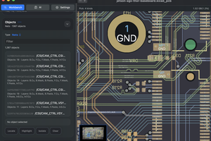
 astroform
 Jarrett
 Jake Robinson