 Stephen Willcock
Development Roadmap
Phase 1: SPI Display Interface (complete)
Expansion board with 7 hardware SPI interface "slots", initially using the first slot for the RA8875 TFT display controller. This enables text/graphics output on a colour display. The hardware SPI gives improved performance over a software (bit-banged) SPI implementation. Whilst this phase is complete - it needs revisiting to make the SPI design more reliable.
Phase 2: Cartridge Storage (in progress)
Removable flash cartridge system for program and data storage, eliminating dependency on a USB host computer for standalone operation - load from cartridge, save data / state to cartridge, swap programs without external tools.
Phase 3: System Redesign
Complete revision of all the boards - BeanZee, BeanBoard, and SPI interface incorporating lessons learned. Unified design, optimized PCB layouts, and some form of enclosure yet TBD.
Core Components
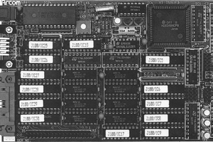
- BeanZee Z80 SBC
- BeanBoard QWERkY keyboard / GPIO
- BeanBoardSPI SPI interface board
- 800x480 TFT display panel with RA8875 controller
- Cartridge slots for removable flash storage
- Integrated battery power supply and enclosure
Technical Details
The BeanZee CPU board has a 10MHz Z80, 32K ROM, 32K RAM and a UM245R USB module. There is an onboard monitor program (Marvin) which supports multiple consoles for input/output - e.g. USB and BeanBoard keyboard, LCD display and colour TFT display. Marvin also integrated RT Russells Z80 BASIC.
The BeanBoard MX mechanical keyboard implements an 8x8 matrix electronically - which is scanned directly by the Z80 - and is physically arranged as 16 columns by 4 rows, providing a sort-of traditional QWERTY layout. It also has a 20x4 character LCD display and includes an 8-bit GPIO for experimentation and interfacing.
BeanBoardSPI interface uses a 74HCT299 universal shift register for input and output. This dedicated board has 7 SPI channels, and eliminates GPIO bit-banging (improving performance), and was done specifically to make the TFT display more usable. However, there are timing issues relating to the synchronous nature of the '299 and this board needs a redesign.
An Adafruit RA8875 TFT controller board is connected via the hardware SPI. This provides a 7.0" 800×480 pixel colour text and graphics display.
A cartridge system provides removable flash storage, allowing multiple programs with data on removable media - a key feature making BeanDeck a proper self-contained computer. This is not banked ROM, but rather programs and data are transferred to and from cartridge "drives" to RAM via the Marvin monitor.
Software Support
Marvin monitor provides a basic console, either over USB or the BeanBoard peripherals, and is able to load and execute programs, or inspect memory. It has been extended with a BASIC interpreter and an RA8875 driver. A driver for the flash cartridges and a simple file system are currently in development.
Sponsorship
This project is sponsored by the helpful folks at PCBWay who are providing PCB manufacturing for the BeanDeck system boards. I appreciate the support they are providing.
 Keith
Keith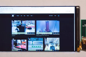
 twl
twl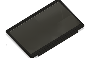
 John Basista
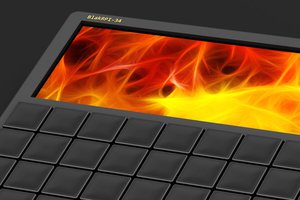
 pcadic