 Stephen Willcock
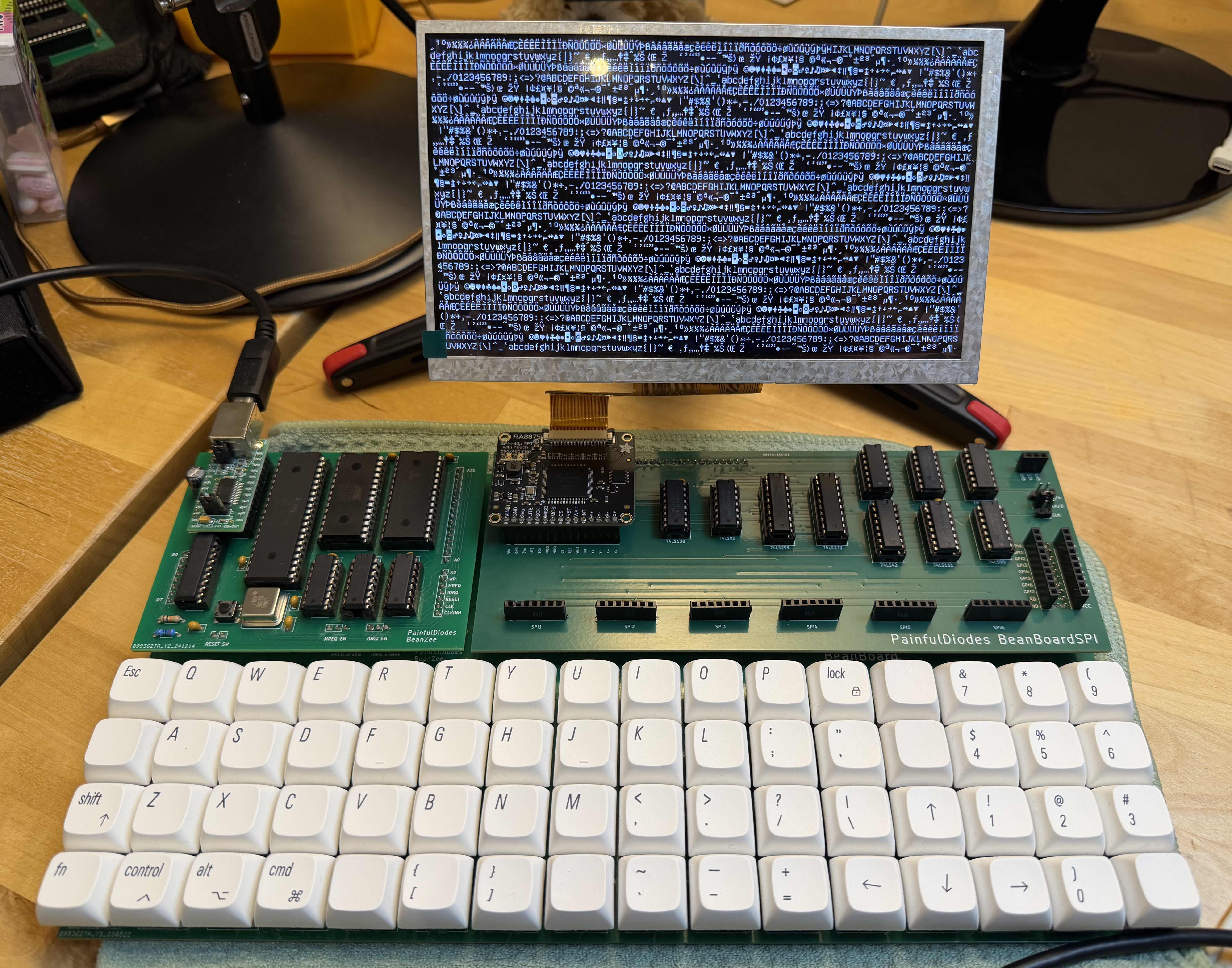
The BeanBoadSPI PCB is now assembled and tested working with a RA8875 controller and TFT display panel. I puzzled over timing for a couple of weeks... turned out to be a design flaw hiding in plain sight...
PCBs arrived from PCBWay - who have kindly sponsored this build - five copies of a 200x80mm four-layer board, looking clean. Assembly was straightforward: ten DIP sockets, seven SPI connectors, jumpers for clock selection, decoupling caps throughout, and the BeanBoard edge connectors. Nearly done when I discovered I was missing a 74LS02 (NOR gates) - not in my parts box. A few days' wait for an RS order, then it went in and the board was ready.
First test was a Z80 loopback: read a char from the console, send via SPI, read back, echo. With MOSI and MISO bridged, whatever goes out should come straight back. It didn't work reliably with the clock divider set up as it had been on breadboard: CLK/4, but switching to full speed (CLK/1) worked perfectly - CLK/2 too. I noted it as odd and moved on. That was a mistake.
Adapting the RA8875 display driver to use hardware SPI in place of bit-banging confirmed the problem. CLK/4 fails with "RA8875 error", CLK/2 works. CLK/1 fails again. Slower is worse - which makes no sense on the surface.
Debugging was methodical but took longer than it should have. Software delays made no difference. My oscilloscope confirmed all three clock signals were present and correct on the jumpers. A register dump from the RA8875 showed register 0 coming back correctly but everything after it as garbage, in a suspiciously regular repeating pattern.
I tried resetting the clock divider flip-flop on each write, reasoning that the free-running divider phase might be causing the RA8875 to see unexpected edges. In simulation this appeared to help, but wiring it into the full simulation killed all serial output entirely - resetting the flip-flop on /WR holds the divided clock low throughout the write cycle, so there's no rising edge to trigger the 74HCT299's synchronous load.
That was the lightbulb moment. The 74HCT299 only captures bus data on a rising clock edge - not when the load signal is asserted. At CLK/2 the Z80 write pulse is long enough that a rising edge always falls within it. At CLK/4 the edges are 400ns apart and the write pulse ends first. The shift register never captures the new data and quietly retransmits whatever was already in it. Because the divider runs freely this is intermittent in general, but becomes a consistent pattern when software loops regularly - hence the repeating garbage in the register dump.
This is a design flaw. I'd noted the synchronous load but didn't fully think through the timing implications at divided clock speeds. My simulation didn't model the Z80 write pulse width accurately; I was stepping through manually. Real hardware found the problem for me.
For now CLK/2 works well enough to keep development moving. The design will need a revision before CLK/4 is usable.
Full write-up on the blog: [link]
Discussions
Become a Hackaday.io Member
Create an account to leave a comment. Already have an account? Log In.