Close
0%
0%

Hybrid MicroElectronics-Factory 3D Printer

In-Situ Synthesis of Conductive Nanomaterials via Tool-Changing system on an FDM corexy 3D printer.

Similar projects worth following
As a Mechatronics student in the Dominican Republic, I wanted to build an Ion Drone which required a custom planar flyback transformer and later attempted to miniaturize a pair of AR glasses for my university capstone project. In both cases, I hit a wall: getting a custom PCB meant waiting 3 weeks for shipping from China. That delay kills creativity.

In underdeveloped countries, innovation is paralyzed by logistics. While we study advanced concepts like Quantum Computing and Plasma Physics, we lack the nanotechnology facilities to build the hardware. Existing solutions like NanoDimension or Voltera are priced for Fortune 500 companies ($50,000+), not for students. I realized that to solve this, I couldn't just buy a printer; I had to build a platform capable of manufacturing custom electronics locally, instantly and cheap.

The Solution:
I am building an open-source Hybrid Tool-Changing Platform that integrates six distinct manufacturing processes into a single automated workfl

Hybrid Tool-Changing Platform 

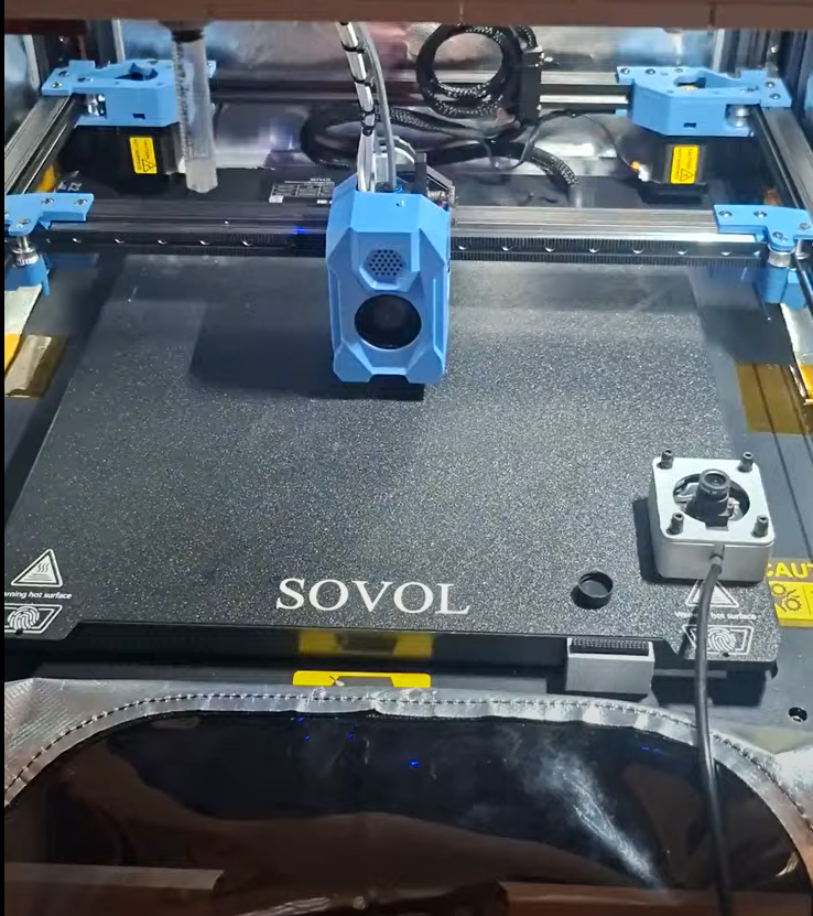
Consisting in a 3d printer that integrates six distinct manufacturing processes into a single automated workflow by using a toolchanger for printing/assembly electronic hardware:

  1. Structural FDM 3d Printer extruder: High-temperature extrusion of engineering thermoplastics (ASA/PC) to create the chassis and dielectric layers..
  2. Laser Sintering (10W): used for the in-situ reduction of metal-oxide inks, synthesis of Laser-Induced Graphene (LIG), and precision cutting/engraving of masks.In-situ reduction of Copper Oxide inks and synthesis of Nickel-Graphene sensors (LIG), laser engraving and cut.
  3. (Future goal/ outscope / pending) Direct Ink Writing (DIW): Precision dispensing of conductive pastes using syringes or inkjet cartridges.
  4. Wire Embedding: Automating the embedding of twisted-pair copper wire for high-current power rails and data lines.
  5. (Future goal/ outscope / pending) Pick & Place: SMD placement of commercial silicon components.
  6. (Future goal/ outscope / pending) In-Situ Etching: Laser-masked acid etching for high-precision copper PCBs directly on the bed.
  7. Drag knife tool / Pen Holder: for cutting copper foil if used or painting silk mask over tracks.

Real-World Impact: Active Composite Structures 

This platform brings a new idea to life: electronics where the circuit is the structure. It enables:

  • Academic / Scientific Hardware: Printing multilayer PCBs, custom RF antennas, Graphene Oxide P-Bit arrays for Quantum emulation, electrodes for Hydrogen electrolysis, mems microfabrication and sensors.
  • Consumer Goods: Creating prosthetics with intrinsic geometry motors and batteries embedded inside the plastic, or smart wearables with sensors printed on fabric.

Furthermore, this hardware lays the foundation for Generative AI to not just design, but physically manufacture complete electromechanical devices without human assembly. My goal is to deploy this technology at the INTEC University Mechatronics lab, creating a pilot Micro-Fabrication facility that allows students to bring unique designs to life immediately.

Material Science Innovation (The "Open Ink" Initiative)

A core component of this project is the development of open-source chemical recipes that replace expensive consumables with synthesized "Reactive Inks." These materials are designed specifically to interact with the machine's laser and dispensing architecture:

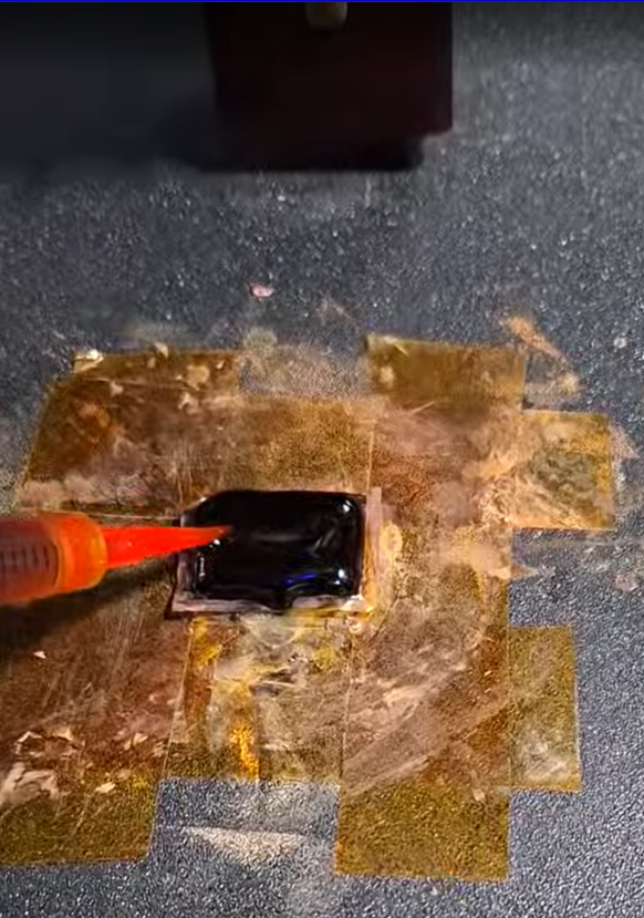
  • Copper Oxide Ink (The "Liquid Wire"): A low-cost formulation of Copper(II) Oxide nanoparticles, Ascorbic Acid (Vitamin C), and binders. When exposed to the 450nm@10W laser, the Vitamin C reduces the oxide, instantly transforming the black paste into highly conductive Pure Copper traces.
  • Nickel-Sugar Ink (The "Graphene Generator"): A composite of Nickel powder and Sucrose. Upon laser irradiation, the Nickel acts as a catalyst to convert the sugar into high-quality Graphitic Carbon/LIG. This material is optimized for printing sensors, supercapacitor electrodes, and thermal noise sources for quantum emulation.
  • Graphene Oxide (GO) Ink (The "Digital Switch"): A specialized ink used for create memresistors, mosfets, diodes and transparent electronics. 
  • Etching Chloride Gel (The "Subtracter"): A modification of Ferric Chloride using Xanthan Gum. This transforms liquid acid into a stable, printable gel. It allows the printer to selectively etch copper foil directly on the build plate without risking damage to the motion system, enabling high-resolution subtractive manufacturing.

More info can be found in the following white paper in progress>

Project Overview

Fusion 360 file here> https://a360.co/4shNm0m

Modular Dock File here> https://a360.co/4rANtCX

This version is with the wire embedder, but the microscope dock and second extruder is hidden.

This version is> https://a360.co/4cQAOYY

Wire Embedder model here> https://a360.co/4bsdkH0

Edited by Google Gemini
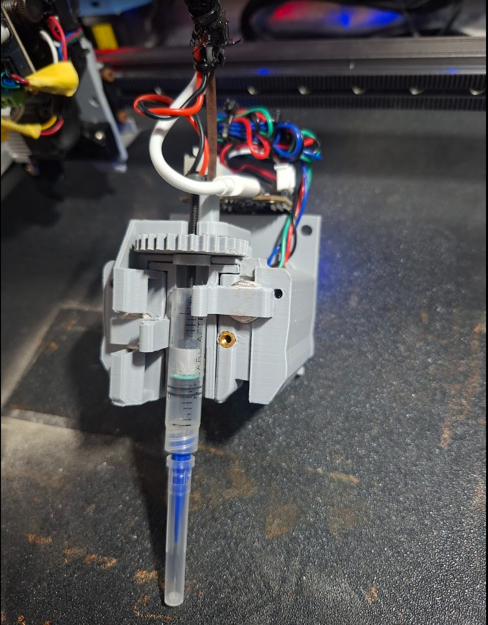
  • Dispenser Redesign and PnP Tool

    Joanbelk08/22/2026 at 18:20 0 comments

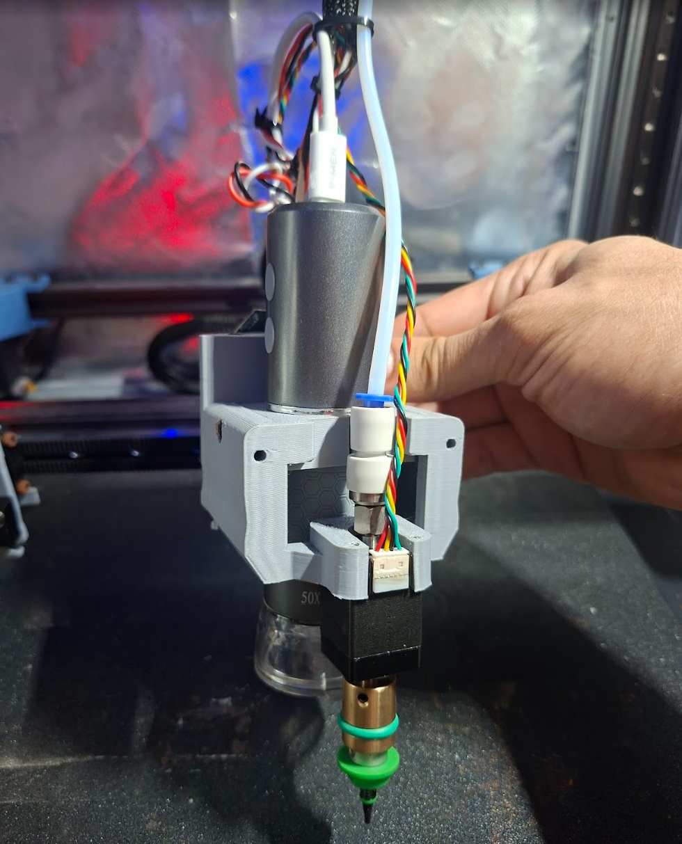
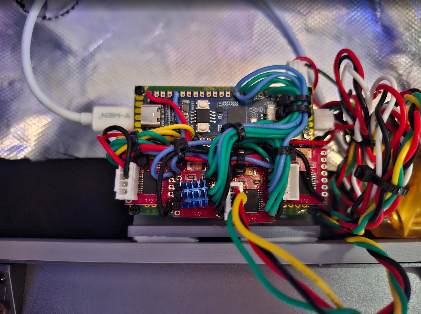
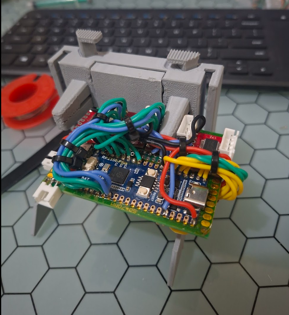
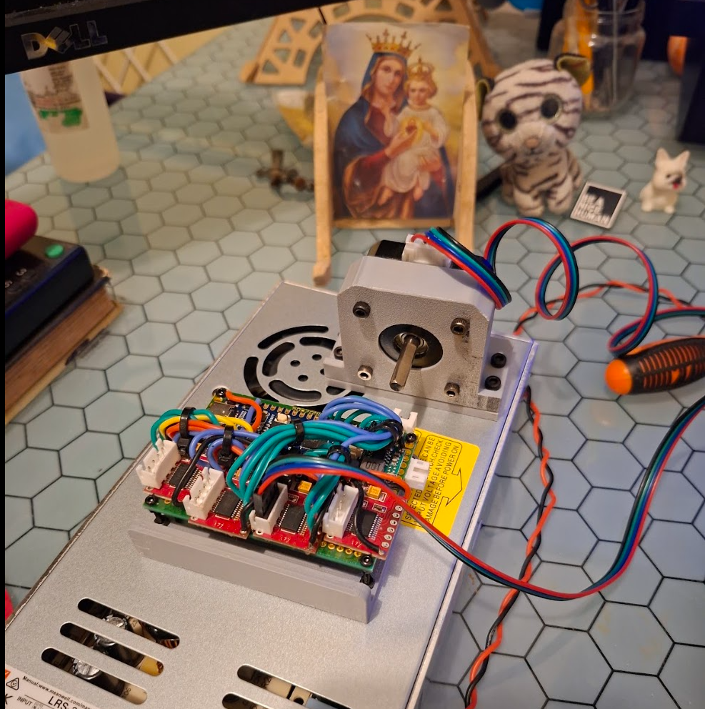
    In the last month I spent time prototyping a protoboard circuit for controlling a PnP nozzle stepper motor, a vacuum pump and a coil winding stepper motor addon.

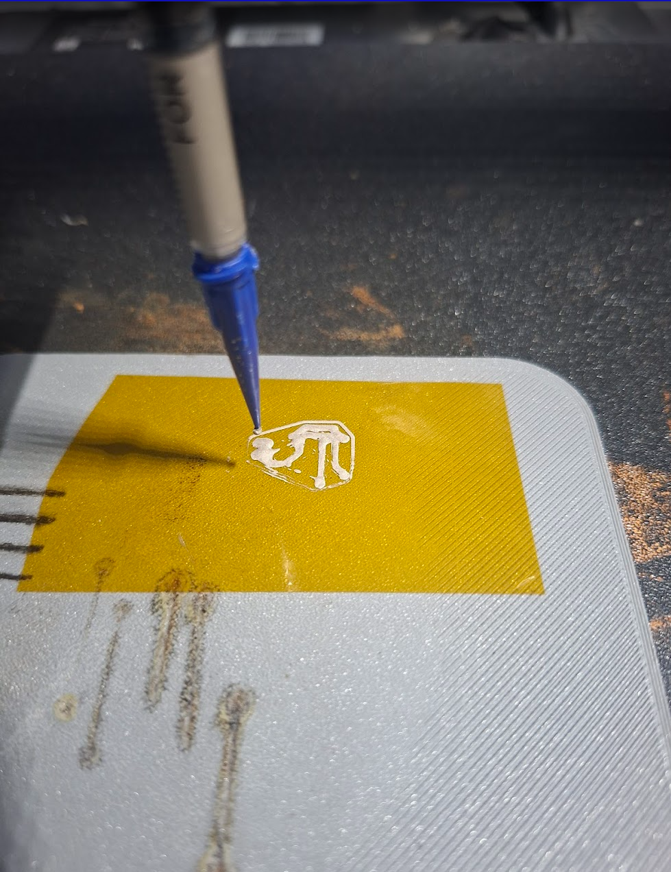
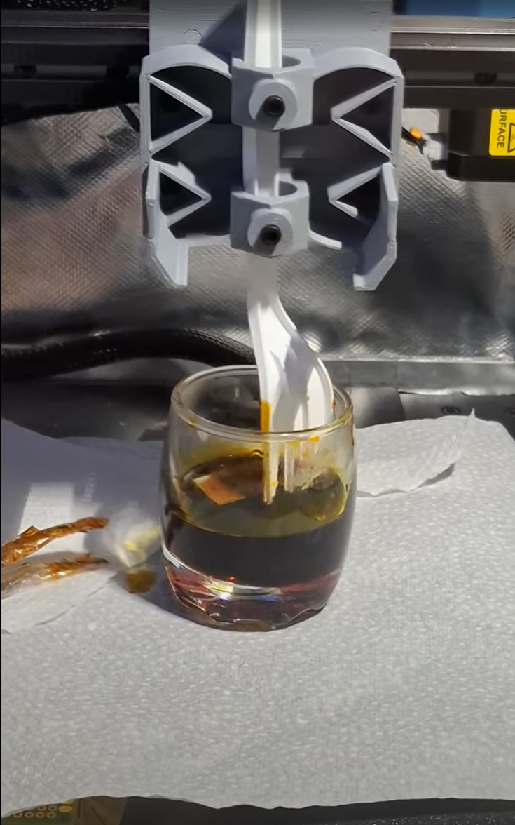
    Also redesigned the syringe extruder to seems more like the Voltera dispenser with a quick disconnect Syringe mechanism and before building the new model, I discovered that calibrating the extruder with a Syringe is the same as calibrating the 3d printer Extruder in orca slicer, although I used custom G-code tests written by Gemini. First, I needed to do a flow test, then a Pressure Advance Test and finally a Retraction Test. But happened that the ink I used dried fast exposed to air and the nozzle constantly clogged. This was resolved by adding some skirt before printing, and maintaining the nozzle capped with a bit of acetone inside when not used.

  • PCB Test using Copper Tape

    Joanbelk06/29/2026 at 14:19 0 comments

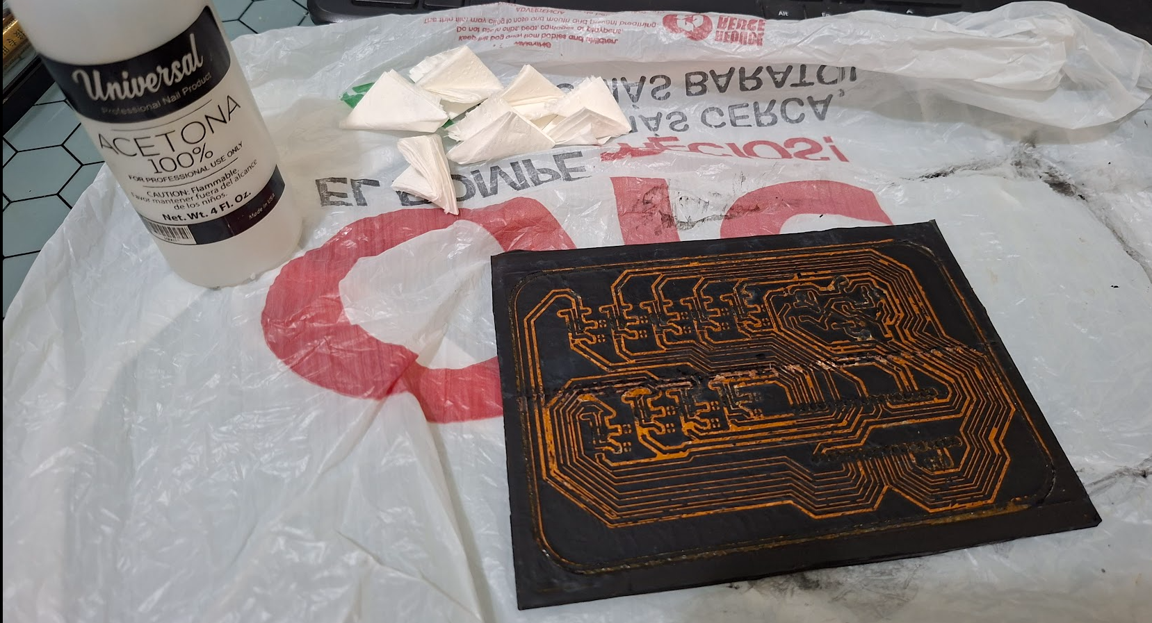
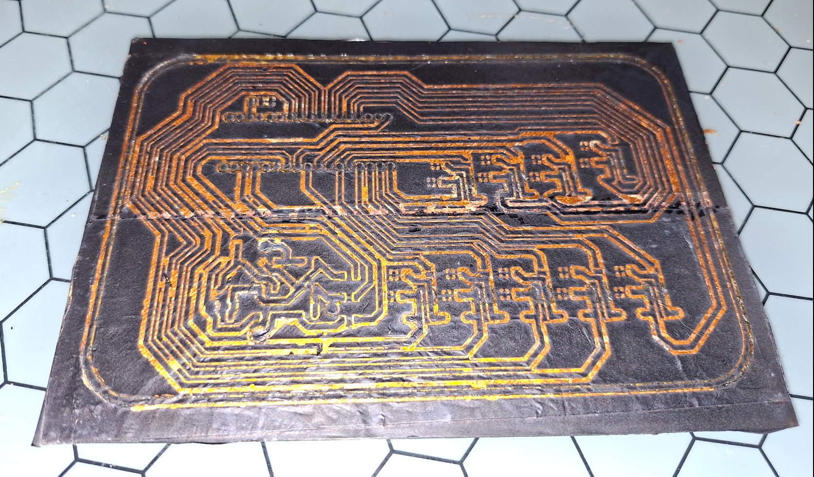
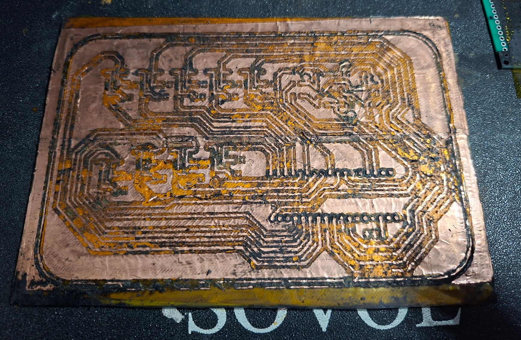
    I have been using copper tape and kapton tape on a ASA printed base to create a PCB aproximately 10x10 cm in size. Due to poor copper adhesion, the copper glue and overetching has been very difficult for me to create a working PCB. Most of the copper dismantled while cleaning the paint with acetone. 

    I will try next to use adhesive transfer tape and copper foil, but i have to wait it arrive from amazon.

    I was following this process:

    Copper Tape Process
    1. 3D printer ASA Base
    2. Layer Kapton
    3. Copper tape 1 Layer
    4. Paint Copper
    5. Laser
    6. Etch ink bottom layer
    7. Clean
    8. Kapton over
    9. Laser drill vias
    10. Conductive paste
    11. Copper tape over 2 Layer
    12. Paint Copper
    13. Laser engrave
    14. Etch ink top layer
    15. Clean
    16. Kapton Tape
    17. Laser drill pads.
    18. Plot silkscreen with pen holder.

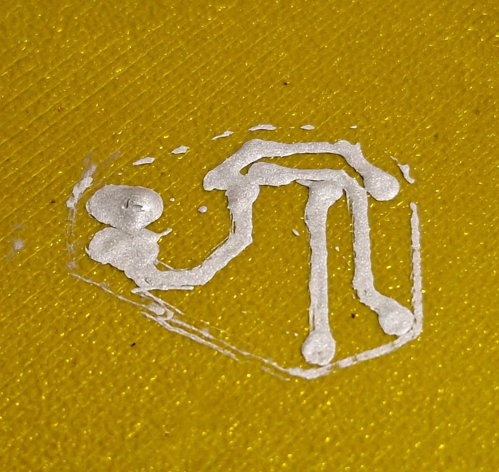
  • Direct Ink Writing Test

    Joanbelk06/26/2026 at 14:35 0 comments

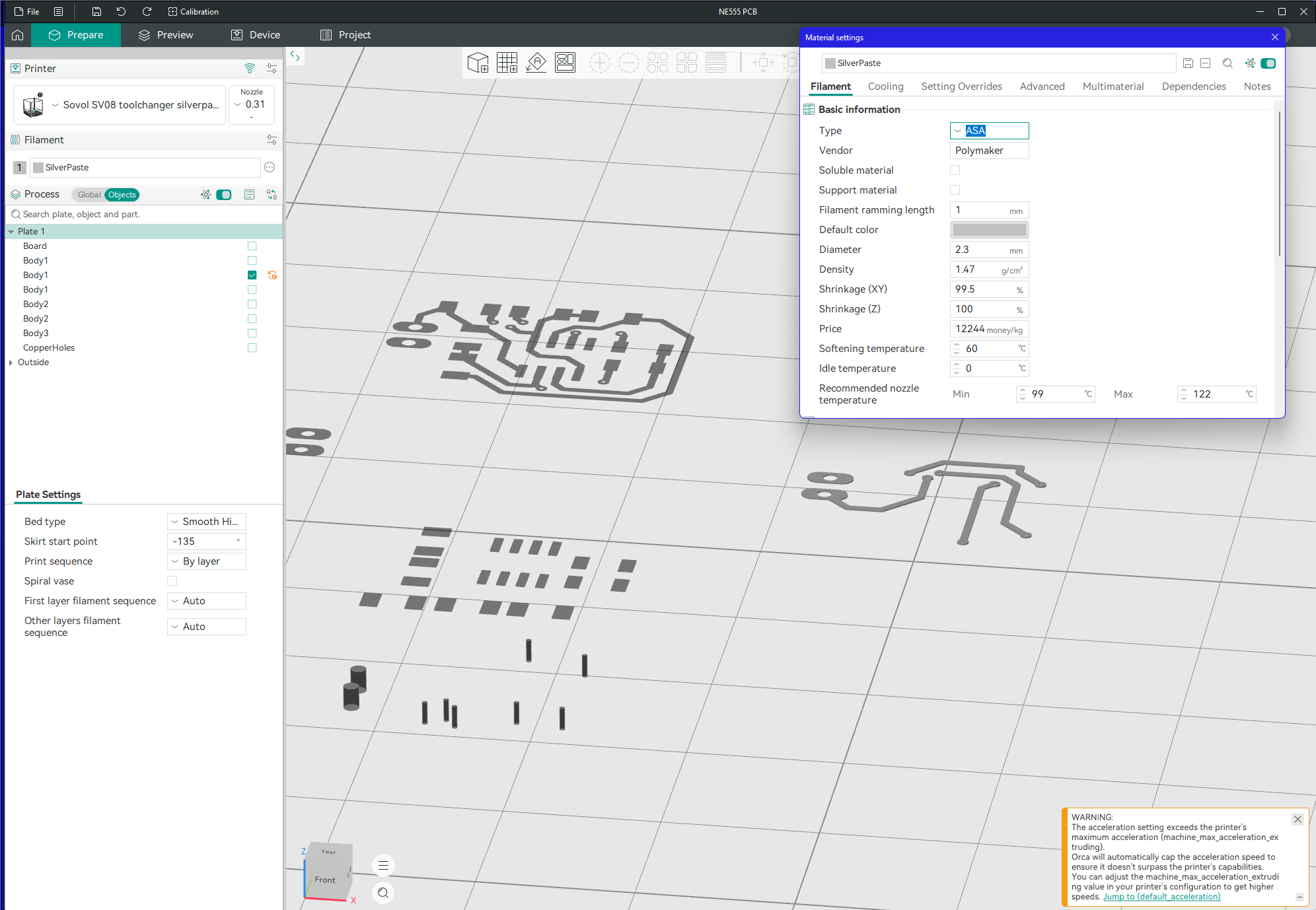
    In the last month I was also testing printing Commercial conductive silver Paste with the syringe. This was a difficult task as I was unexperienced about the fluid mechanics and rheology of extruding paste. I tried adjusting and creating a profile in OrcaSlicer in order to print silver paste as it was FDM filament. Up to date having fine tuned yet the process as I noticied some mechanical problems with the extruder mechanism in my printer. (borrowed from the LumenPnP project xD). 

    The following webinar changed my mind about DIW. I was planning add an Inkjet UV printing>

  • Laser Etch SMD Protoboards

    Joanbelk06/26/2026 at 14:22 0 comments

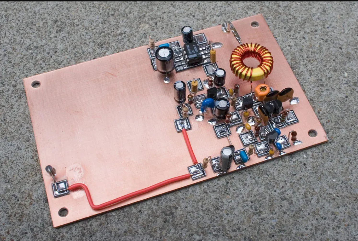
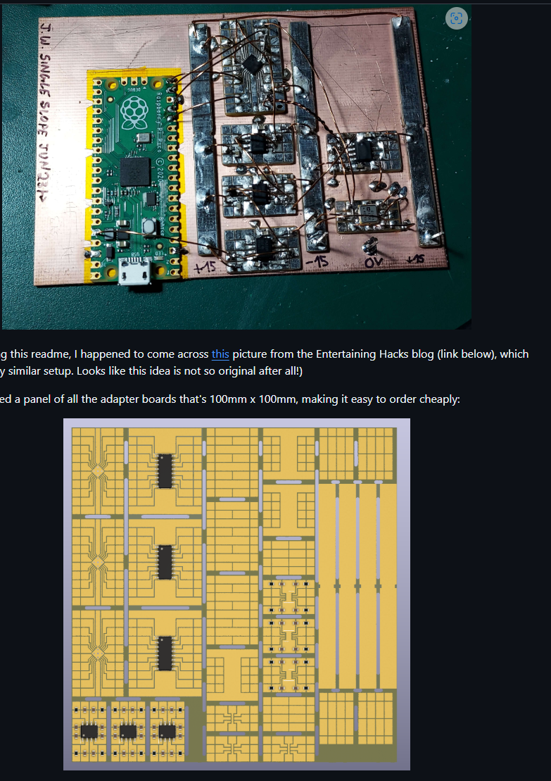
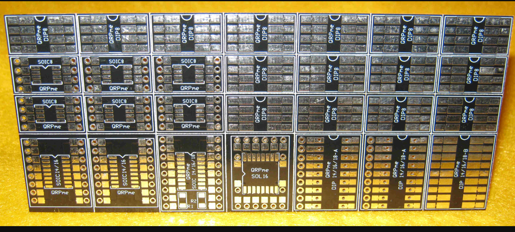
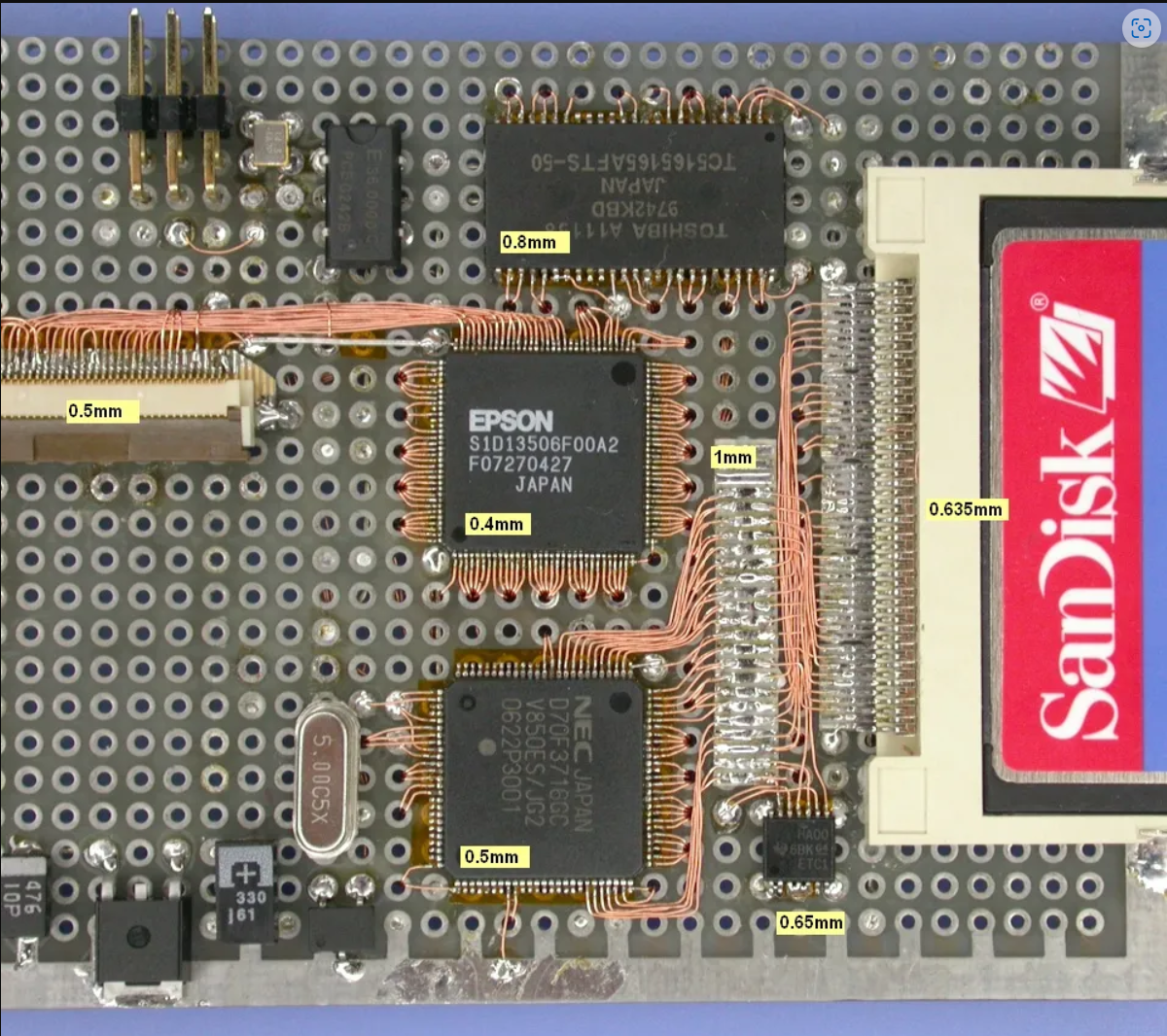
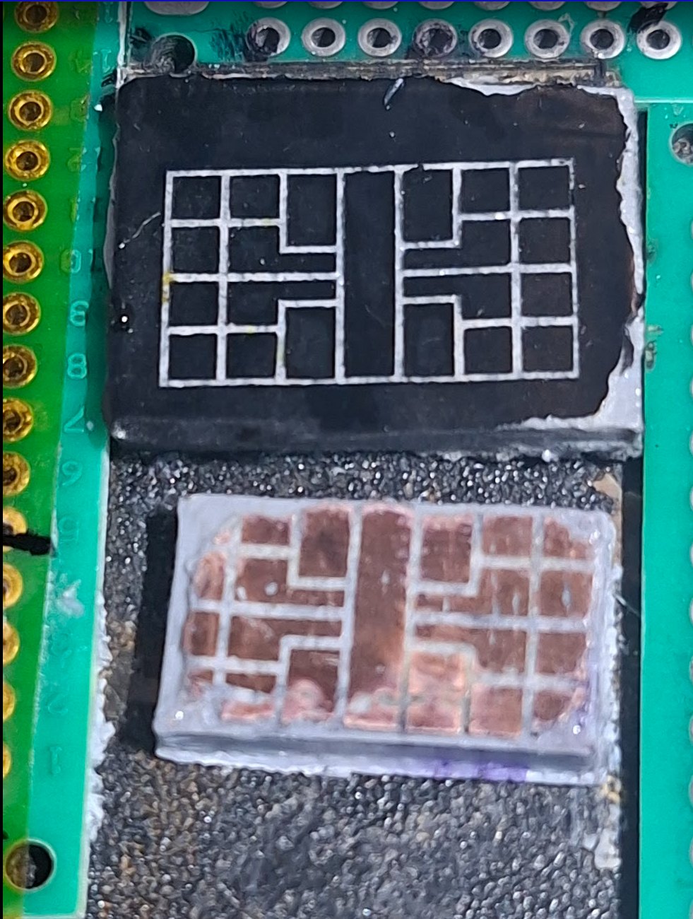
    I am new to PCB prototyping. Searching on the web I discovered many ways people used in the past for rapid PCB prototyping  and I tried to reproduce some by using the Laser Etching. I found the following techniques>

    1. Manhattan Prototyping:

    The WBR – A Simple High Performance Regen Receiver for 40M by N1BYT – Dave Richards AA7EE

    Adapter boards design> NNNILabs/Manhattan-Adapters-Prototyping-Ideas: SMD adapters for Manhattan-style prototyping.

    https://forums.parallax.com/discussion/164493/ground-plane-construction

    2. Wire Bonding like technique>

    Extreme Wiring on the Prototyping Board by NE555

    https://elm-chan.org/docs/wire/wiring_e.html

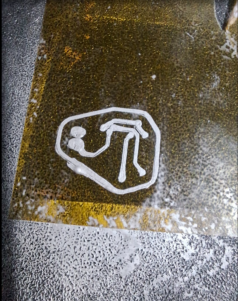
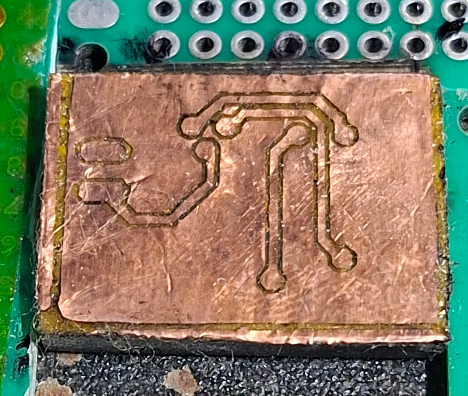
    So, I tried to use Laser Etching by welding with acetone a copper sheet to the ABS in order to create custom SMD protoboard for using as Manhattan Style prototyping.

  • Laser Etching for Ne555 PCB test

    Joanbelk06/26/2026 at 13:55 0 comments

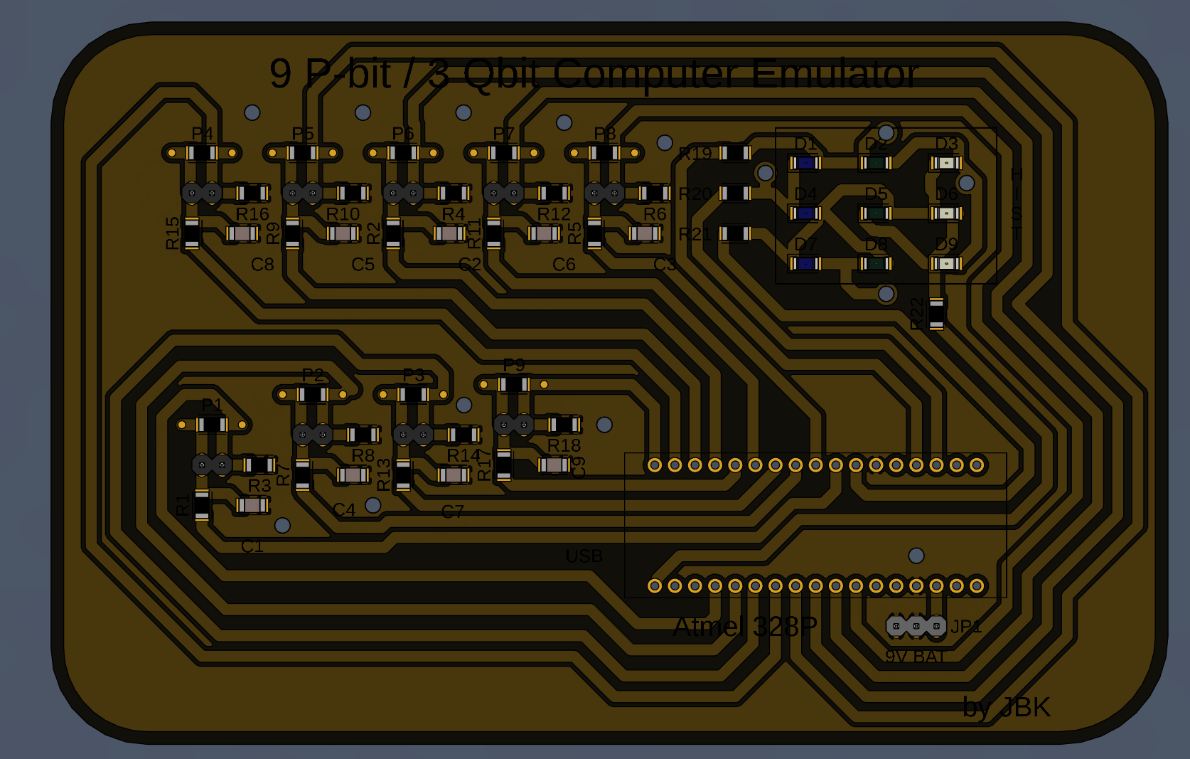
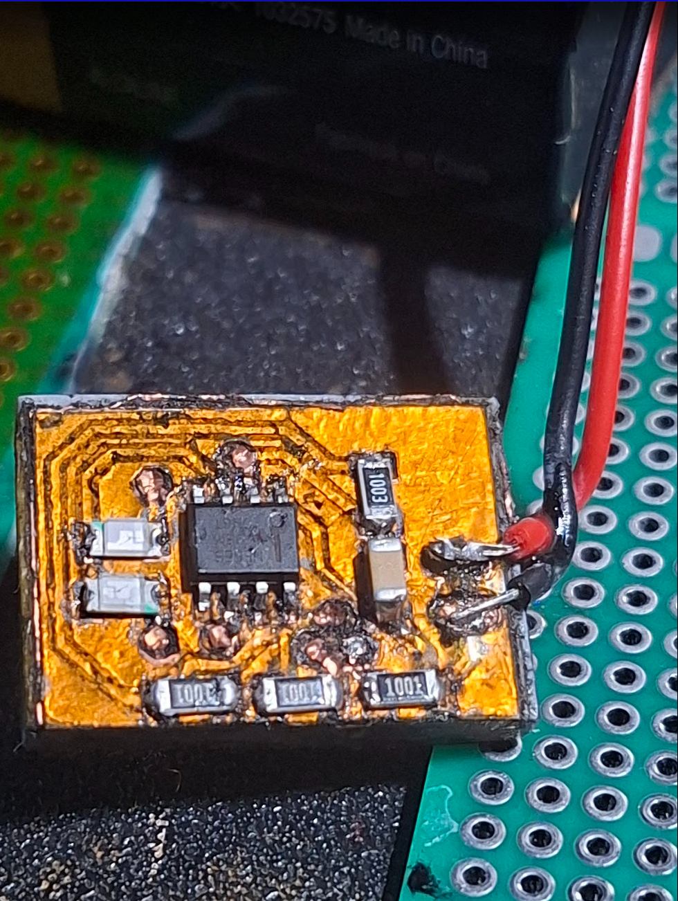
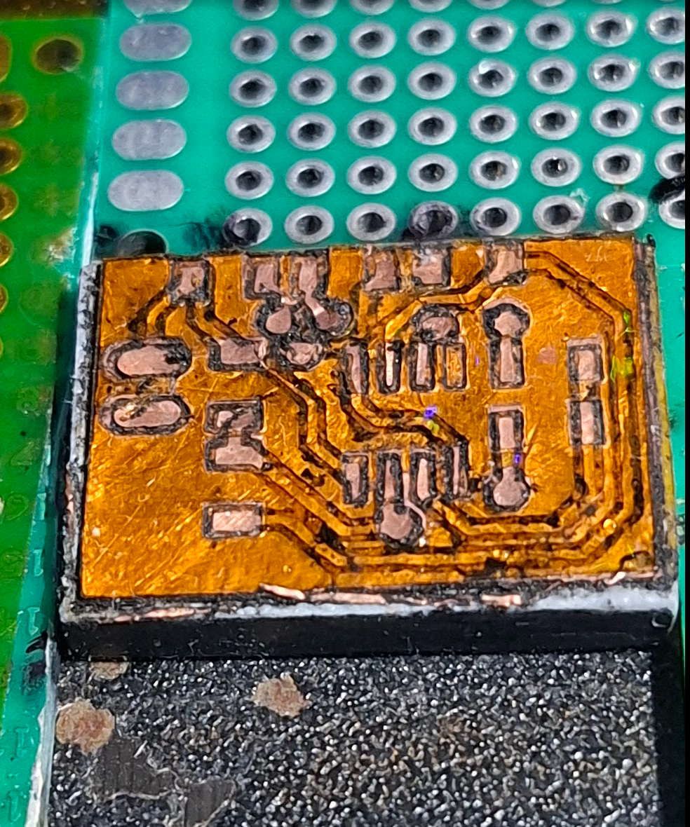
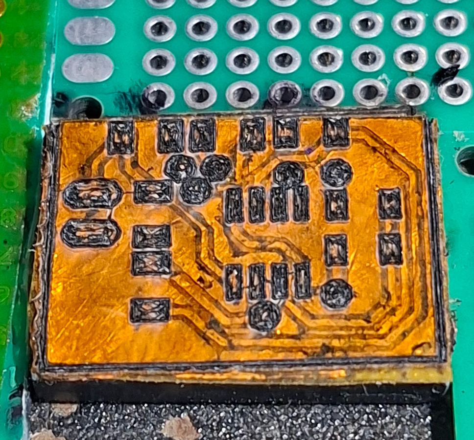
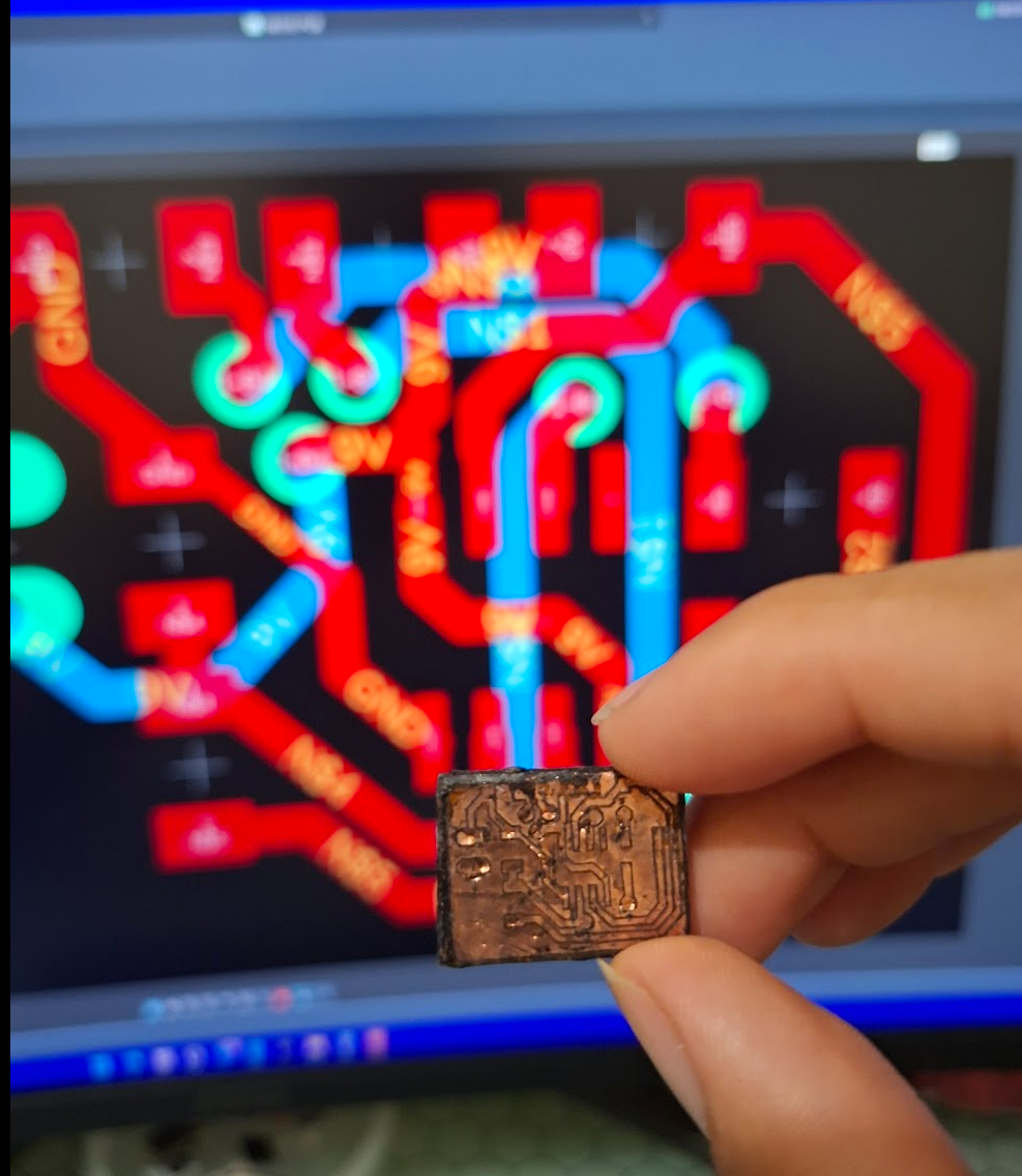
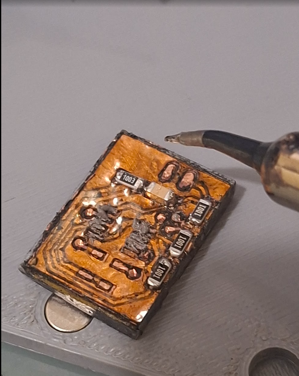
    In the last month I was trying to create a test PCB with 1206 size SMD components and an NE555 IC by creating the smallest PCB trace possible. According to theorical capabilities, the Laser has a pitch of 0.08mm and the Sovol SV08 printer has accuracy of 0.1mm in XY direction. I tried the following:

    1. Laser Etching:

     As I didnt have any experience with laser engraving, had many failures by not using Air assist. I regret using a 10w laser, a 5w laser was sufficient. The idea was to engrave an ink mask over a copper substrate. At the beginning I used acrylic permanent marker and etching gel to avoid taking the 3d printed base out of the printing bed, but happens that the Etching Gel (a mix of ferric cholride with fumed silica) after 20 minutes or more the ink starts to lose grip to the copper surface and ended cutting the small 10mil traces, was also very difficult to optically inspect the board. 

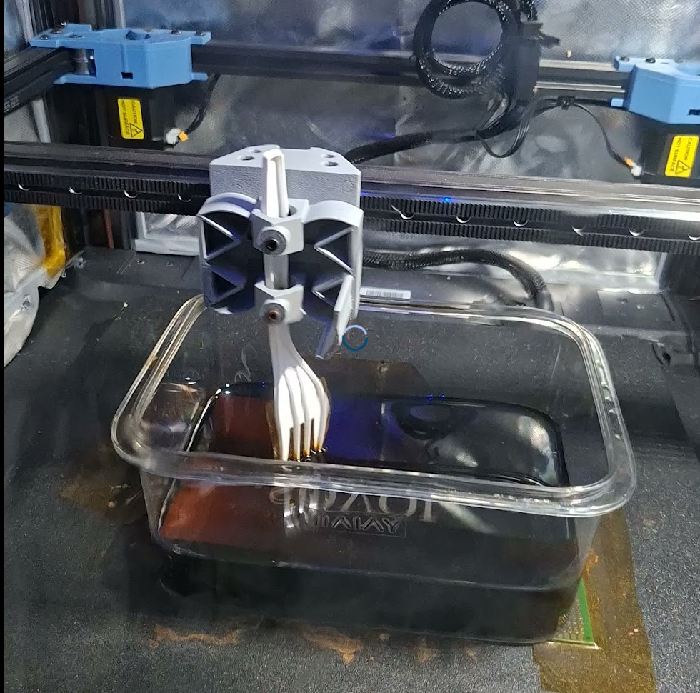
    I ended switching to the classical approach to etch the board in a bath of acid by taking out of the 3D printer Bed. But happens then that when wanting to add more layers insulated by kapton tape over copper tape, as I did not have a fixed plate was difficult to align again the laser. Also for VIAS had to use options like adding solder paste or conductive ink, and Had to use IPA for removing the graphene left by laser milling the kapton tape. For cleaning the paint mask I had to carefully clean by using Q-tips and acetone, one mistake and a trace would be blown away.  Finally after some weeks I was able to create a PCB. Every trace was conductive even through the vias, but after the soldering process with Low Temp Soldering, the circuit may had some shorts and the VIAS where misfriring because I relied in the acrylic tape of the copper tape instead of applying conductive ink. And as time passed I decided to move forward creating another PCB test.

    Agitating the acid etch reduced the etching time from 40 minutes to 15 or 20 minutes, avoiding overetching.

    As reference a similar way for making multilayer PCBs is the following paper although they laser etch the copper with a fiber laser:

    Paper> https://dl.acm.org/doi/abs/10.1145/3374920.3374988

  • Reactive Copper Ink mix Test

    Joanbelk05/23/2026 at 16:28 0 comments

    At this time, following Gemini's recipe for a Reactive Copper ink ended up being very difficult to fine tune for me. Also discovered that I was running my gcode for the laser with Half Speed and ended up burning the ink every time, although not at 10% that is 1W 450nm laser power.

    In theory: If it looks Black and Ashy (Soot that rubs off easily): Too hot. The Vitamin C burned into charcoal; but if the black ink instantly flashes into a Salmon, Bronze, or Penny-Copper color, means it works. 

    The recipe is as following:
     8mL Reactive Copper Recipe
    Part 1: The Carrier Fluid
      5.20 g Ethylene Glycol (approx. 4.8 mL)
      0.60 g PVP K30 (Binder)
      0.20 g Citric Acid 
    Part 2: The Activator (Vitamin C)
     2.00 g Ascorbic Acid
    Part 3: The Metal
     6.40 g Black Copper Oxide (CuO) powder.

    Heat Bed at 85 Celsius for 10 minutes until ink looks bit brown and then fire the laser.

    Is estimated will last for 2 weeks in the refrigerator. 

    But will move on to use copper sheets and etch with the laser instead.

  • Laser Test and Offset Calibration

    Joanbelk05/23/2026 at 16:26 0 comments

    This is a summary of the process followed for calibrating the offset of the main tools (Extruder, Deposition Syringe and Laser). I used the Axiscope software to manually adjust the offset.

  • Toolchanger Tests: Switching Extruder, Laser and Deposition Tool

    Joanbelk05/10/2026 at 02:31 0 comments

    Actual Date> 1-May-2026

  • Toolchanging Tests: Deposition Tool

    Joanbelk05/09/2026 at 23:52 0 comments

    Actual date: 1-May-2026

    After struggling for weeks, finally is somehow stable.

  • Stealthchanger Shuttle Installation

    Joanbelk04/20/2026 at 22:20 0 comments

    Last week I finished wiring the OptoTap Sensor in all electrical tools and installed the Shuttle for toolchanging. I ran on some problems, like not verifying the OptoTap sensor properly working, and also had a electric short with the Optotap sensor in one of the extruders... (doesnt power up now, maybe I will check the buck converter circuit of the micro in the PCB or buy a new one). 

    I hope this week to work in the software to at least record a video of the system automatically switching tools.

View all 30 project logs

Enjoy this project?

Share

Discussions

Similar Projects

Does this project spark your interest?

Become a member to follow this project and never miss any updates