 Pavel
PavelI had started to put together and solder the board, while still designing layout -- this proved mutually beneficial process, as partially assembled board is very good anchor to further design, and having the design slightly ahead of implementation makes adding features a more thoughtful process.
In the process I came to think that there probably will be no 3.3V to 5V logic level conversion on this board (this might be done on separate board that will have to be connected to this one). Also I decided to make VGA output colors RGB222, as RGB332 has trouble with gray color. This decision releases two 3.3V GPIO pins that could be used elsewhere, as Hsync and Vsync signals are also routed to 1.8V bank.
On the other hand, I added connectors for add-on 16-button keyboard (that will block 5 buttons, and be used instead), and for 2 small spi LCD screens, one 128*64 dot matrix display, and other is 320*240 TFT display. They will use the same pins as multiplexed 7 segment display, so, mutually exclusive with it.
---------------------------------------
Here is partially assembled board:
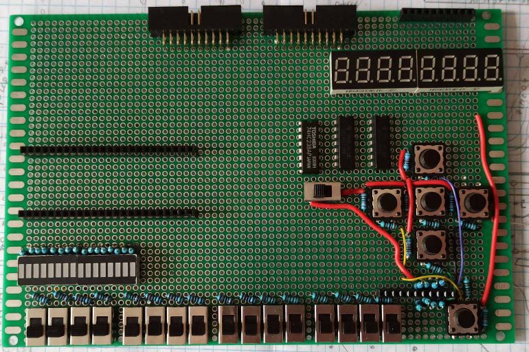
The switches and buttons are already installed and wired, and 7-segment displays are also wired together as multiplexed 8-digit display. The pin header connectors (female) are now soldered by just a couple points each, and still have no wiring connected.
---------------------------------------
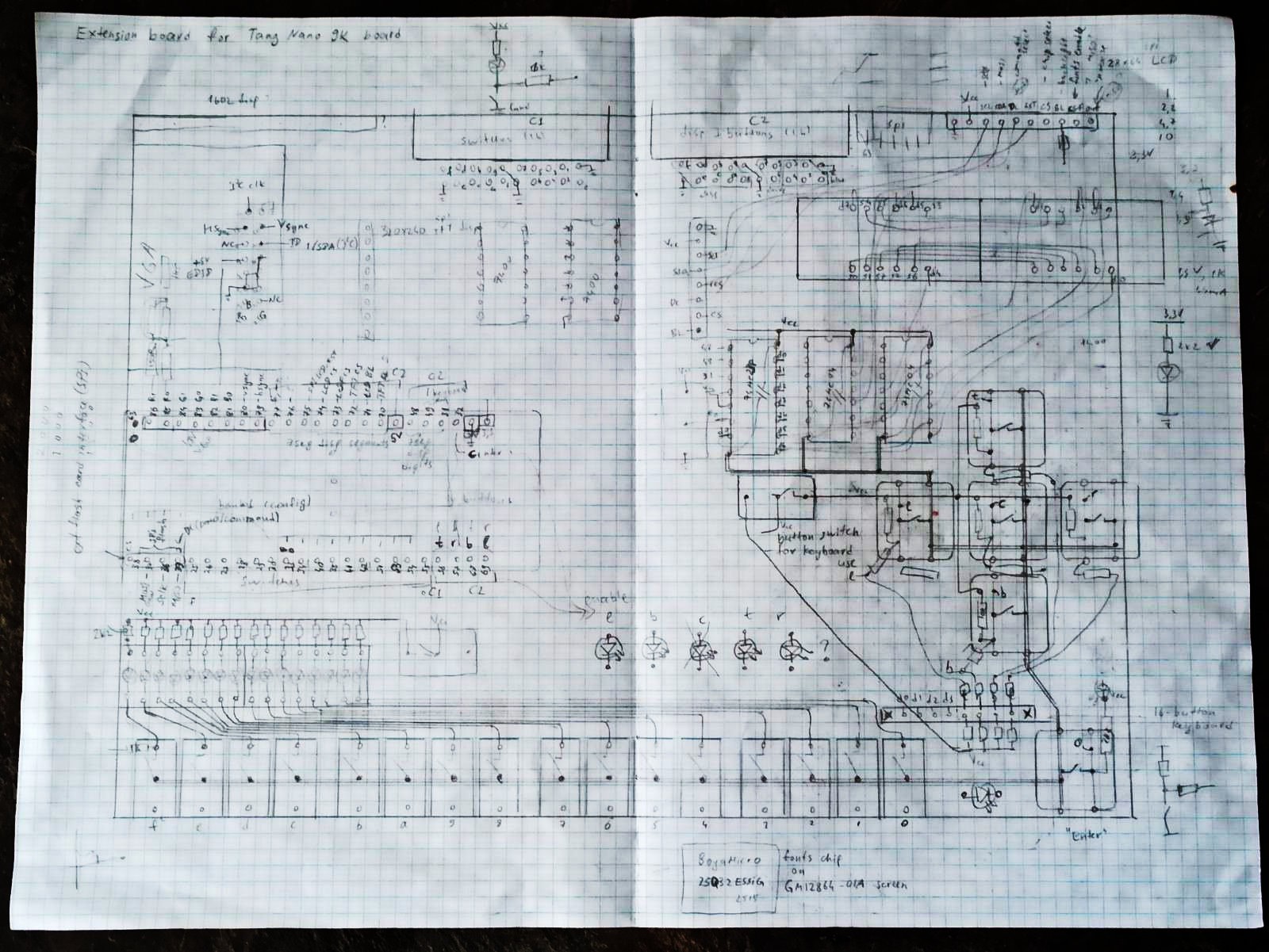
Here is provisional/draft design drawing:
---------------------------------------
Pin assignments diagram:
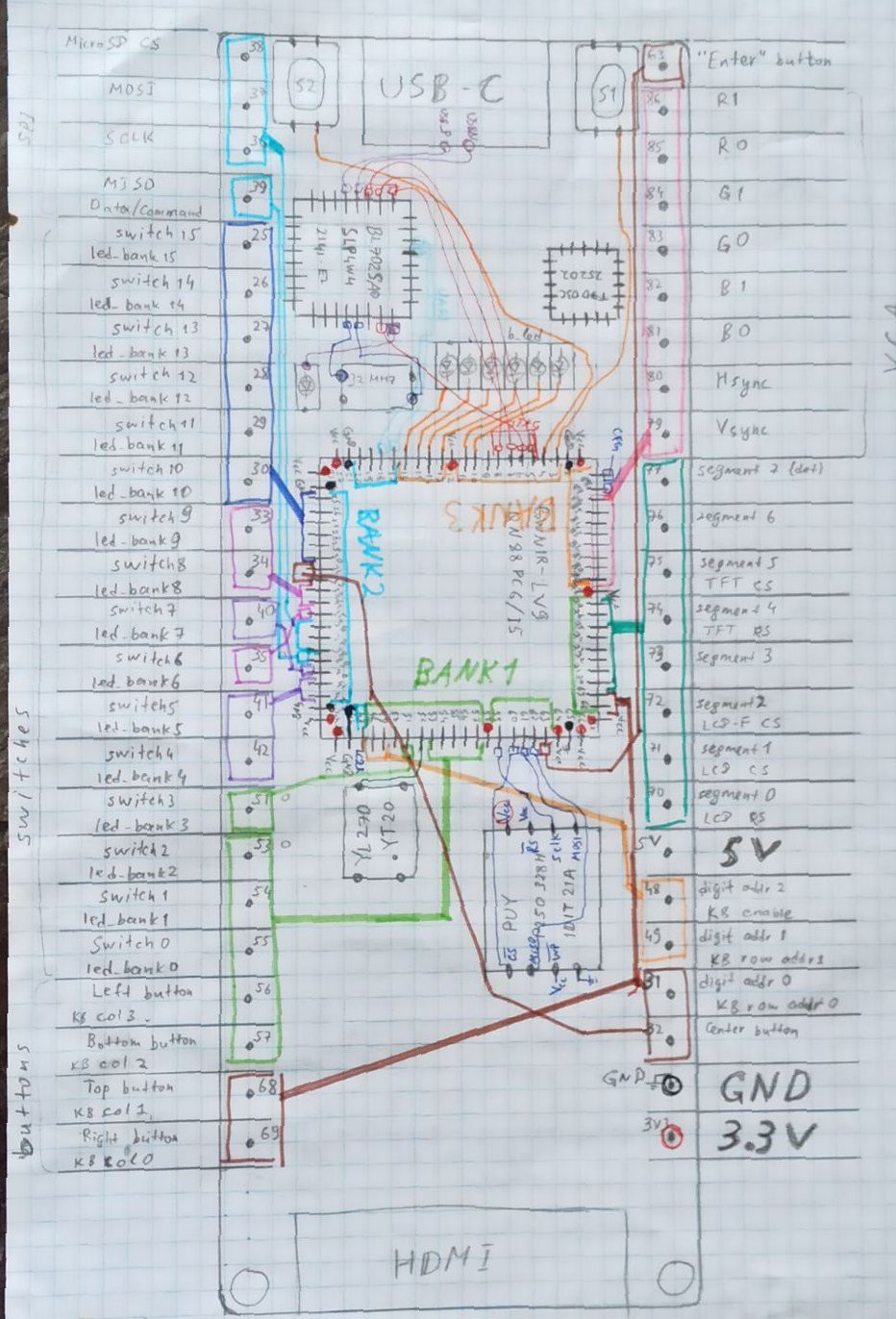 As one can see, on this diagram connections between main fpga IC and board connectors or other devices are traced. This is mostly for more intuitive look-up for writing appropriate .cst files needed for synthesis of Verilog descriptions.
Discussions
Become a Hackaday.io Member
Create an account to leave a comment. Already have an account? Log In.