 Bohan Xu
I have a Youtube video about this project and this is the Intro, Part 1: Program Counters, and Part 2: Registers
0%
0%
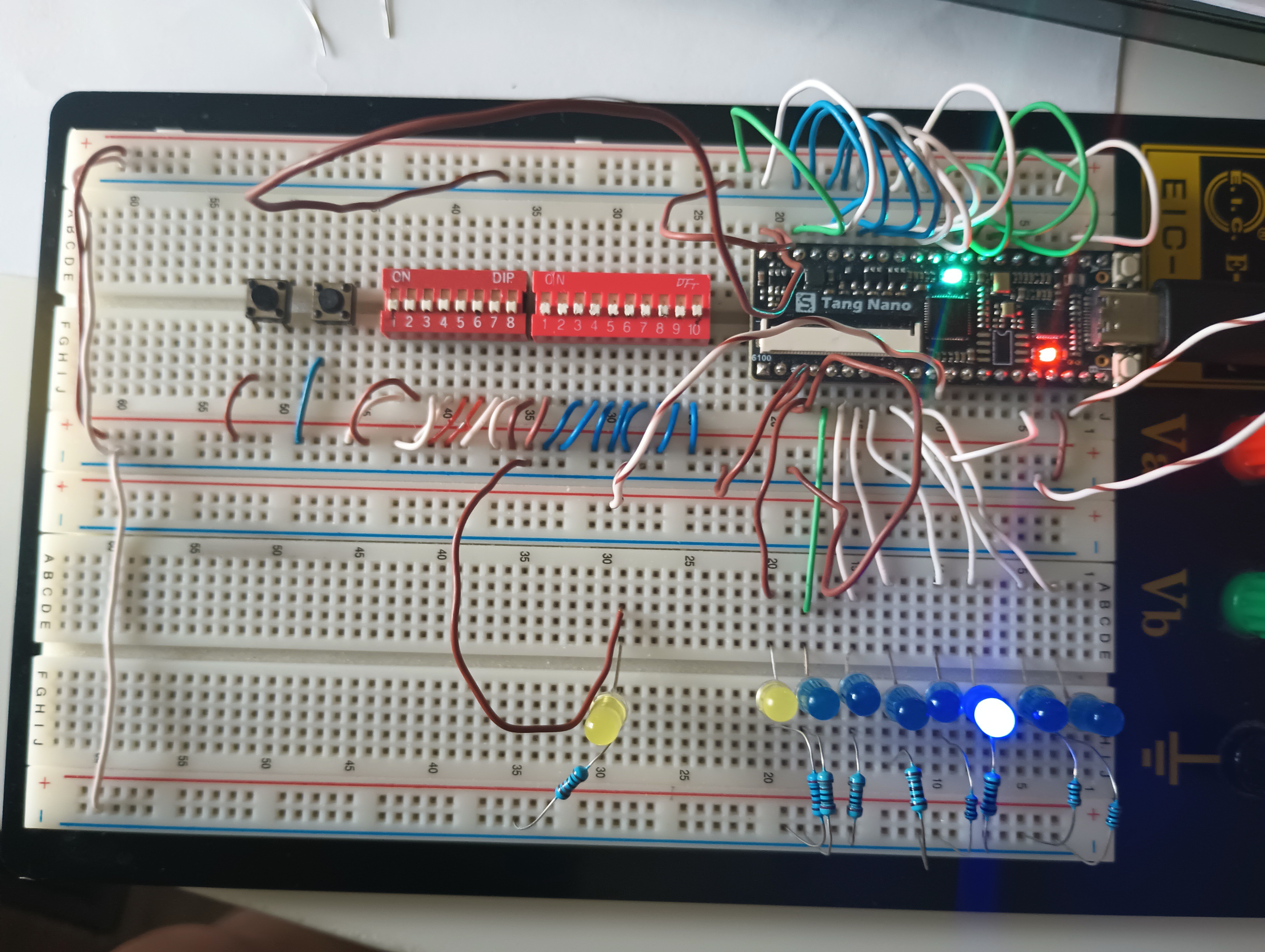
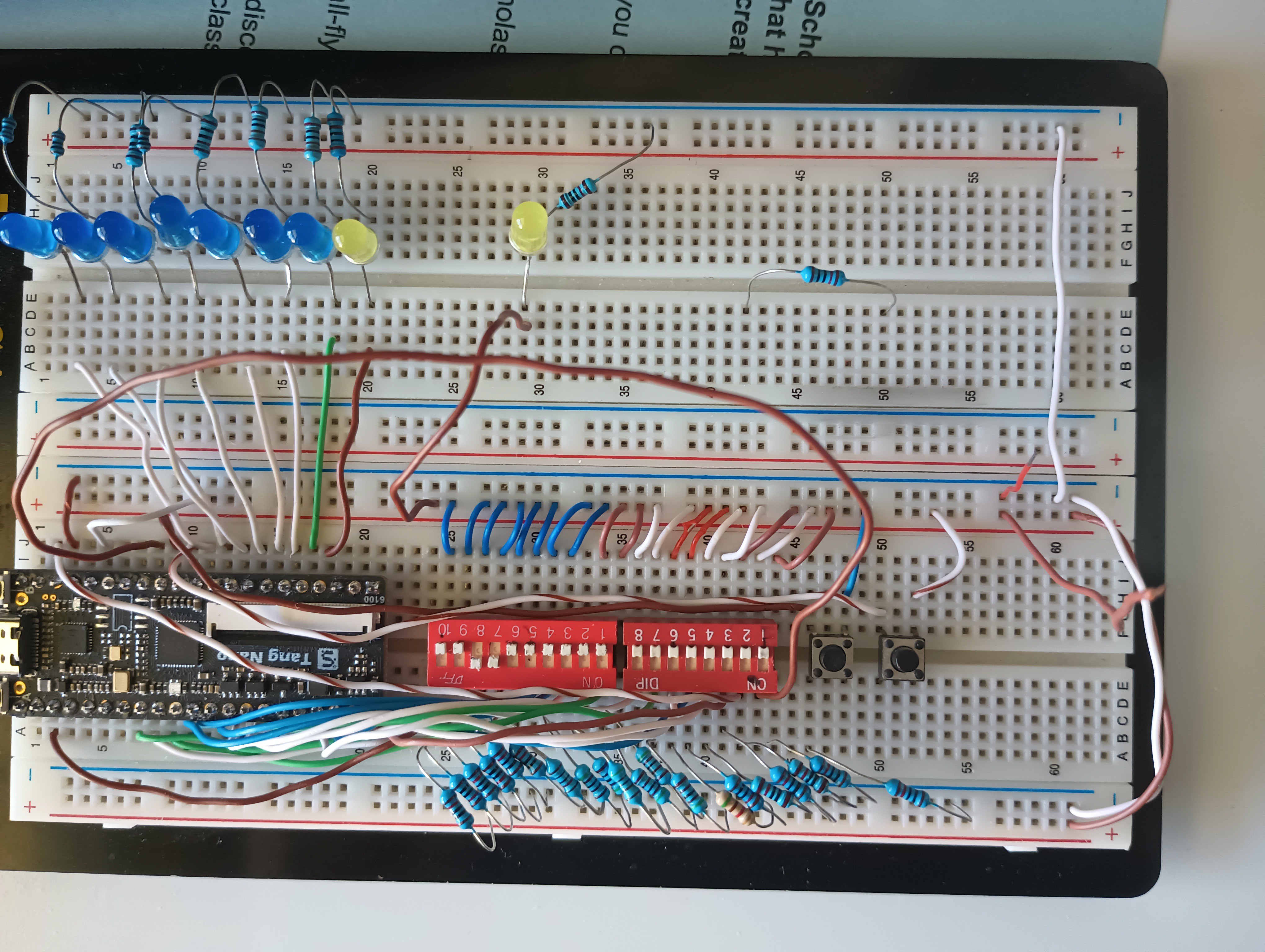
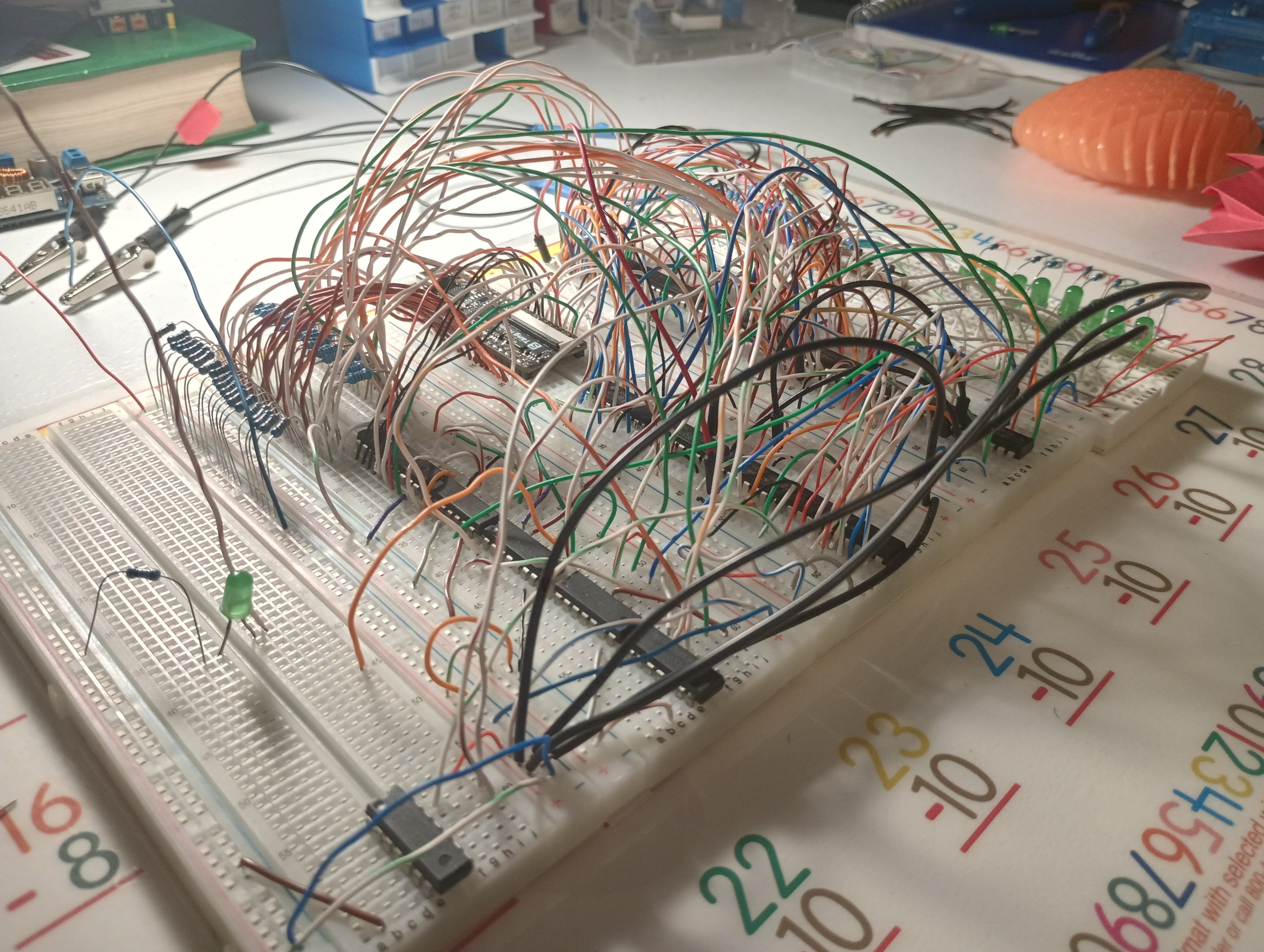
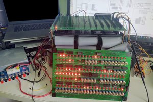
TTL 8-Bit CPU better than Z80
An 8th grader designing and building a real 8-bit CPU from scratch using custom architecture and discrete logic.
Become a Hackaday.io member
Already have an account? Log in.
Just one more thing
To make the experience fit your profile, pick a username and tell us what interests you.
Pick an awesome username
hackaday.io/
Your profile's URL: hackaday.io/username. Max 25 alphanumeric characters.
Pick a few interests
Projects that share your interests
People that share your interests


 Martian
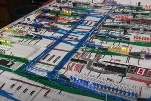
 Fábio Gil
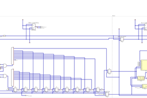
 Augusto Baffa
That’s absolutely amazing for your age!