 roelof4
The presence of a Memory Management Unit is a requirement for multi-tasking operating system such as OS-9 and UniFLEX both of which have many features from UNIX.
Before diving into the details of the CS09 MMU I though it might be good to give an overview of the 3 main approaches to create extra address space (not necessarily MMU)
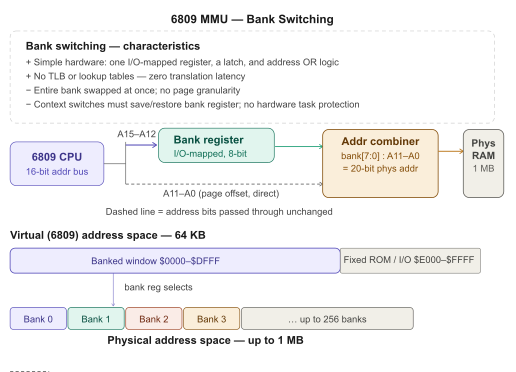
1. Bank switching:
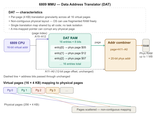
2. Data Address Translation:
3. DAT + task selector:
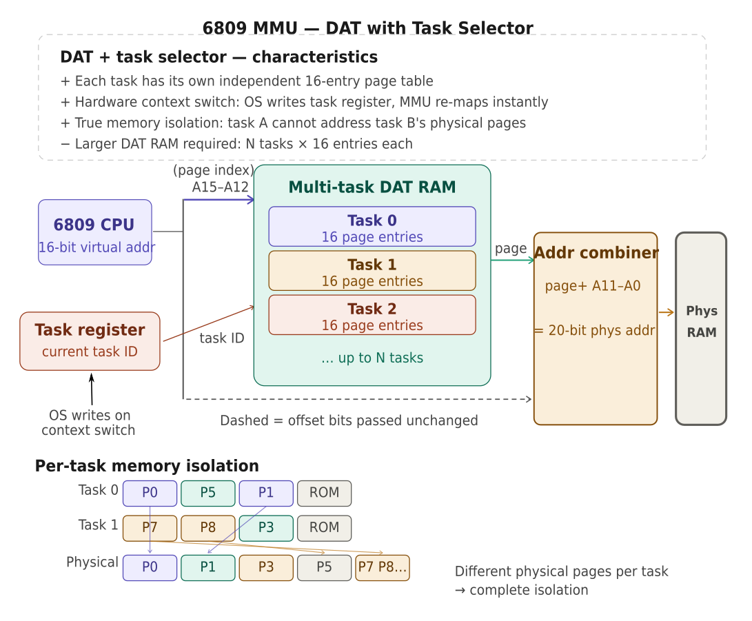
The DAT + task selector gives most flexibility how to structure memory larger than 64kbyte and allows quick switching of the memory mapping of individual tasks without rewriting the DAT RAM.
Often the task register is a physical register (latch) in real implementations which the CPU will update when there is a switching of tasks. The CMS9639 took this concept one step further and introduced a small 4x8bit memory to replace the task register. This allowed 4 sets of task registers that would form:
- System task (task 0)
- User task
- DMA source task
- DMA destination task
Switching between these is automatic and done in the logic chip. So whenever a software or hardware interrupt occurs the System task will be selected and so on.
Below a snippet from the CS09 CPU schematic showing the chosen implementation:
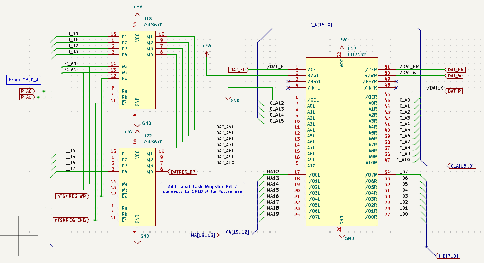
Rather than using a standard 2kbyte RAM memory like the CMS9639, I have followed the approach by Kees Schoenmakers and used a dual-port memory chip (IDT7132). These are fast (35ns) and do away with extra tri-state buffers that are needed for normal memory when switching from MMU use to writing its contents. Here the righthand side of the dual-port memory provides access to its contents (I_D is the internal databus, C_A the CPU address bus). The left side takes CPU address lines A12..15 and the output from the small memory chips and outputs the MMU addresses MA12..MA19 which together with C_A0..11 will form the external address bus.
A set of pullup resistors on MA12..MA19 defines the external bus address before the dual-port RAM has its contents defined and taken out of tri-state. Currently the most significant bit (DATREG7) is not used and connected to the logic chip. In future this could be used to introduce memory write protection.
Motorola did, in fact, develop a MMU chip - the MC6829 - that provides 2kbyte pages. This chip was not long in production and not many copies are around. Unfortunately, the delay in outputting the translated address lines was significant which made operation at 2MHz next to impossible. I know only one commerical machine that used the MC6829, the Positron 9000 (https://binarydinosaurs.co.uk/Museum/Positron/).
Discussions
Become a Hackaday.io Member
Create an account to leave a comment. Already have an account? Log In.